


Core (e200z7) Overview
PXR40 Microcontroller Reference Manual, Rev. 1
13-6
Freescale Semiconductor
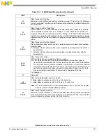
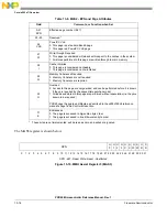
11
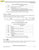
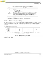
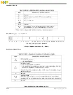
DCWM
Data Cache Write Mode
0 Data Cache operates in writethrough mode
1 Data Cache operates in copyback mode
When set to writethrough mode, the “W” page attribute from the MMU is ignored and
all writes are treated as writethrough required. When set, write accesses are performed
in copyback mode unless the “W” page attribute from the MMU is set.
12–13
DCWA
Data Cache Write Allocation Policy
00 Cache line allocation on a cacheable write miss is disabled
01 Cache line allocation on a cacheable copyback write miss is enabled
10 Cache line allocation on a cacheable copyback or writethrough write miss is
enabled
11 Reserved
This field also controls merging of store data into the linefill buffer while a cache linefill
is in progress. Store data will not be merged when write allocation is disabled. If DCWA
is non-zero, store data merging is enabled regardless of the type
(writethrough/copyback) of write.
14
Reserved
15
DCECE
Data Cache Error Checking Enable
0 Error Checking is disabled
1 Error Checking is enabled
16
DCEI
Data Cache Error Injection
0 Cache Error Injection is disabled
1 Parity errors will be purposefully injected into every byte subsequently written into
the cache. The parity bit of each 8-bit data element written will be inverted. This
includes writes due to store hits as well as writes due to cache line refills.
DCEI will cause injection of errors regardless of the setting of DCECE, although
reporting of errors will be masked while DCECE = 0.
17
Reserved
18–19
DCEDT
Data Cache Error Detection Type
00 Parity Error Detection is selected for both the tag and data arrays Reserved
(defaults to DCEDT=01(EDC) actions)
01 EDC Error Detection is selected for the tag array and parity is selected for the data
arrays
1x Reserved
20
DCSLC
Data Cache Snoop Lock Clear
0 Snoop has not invalidated a locked line
1 Snoop has invalidated a locked line
Indicates a cache line lock was cleared by a snoop operation which caused an
invalidation. This bit is set by hardware and will remain set until cleared by software
writing 0 to this bit location.
21
DCUL
Data Cache Unable to Lock
Indicates a lock set instruction was not effective in locking a cache line. This bit is set
by hardware on an “unable to lock” condition (other than lock overflows), and will
remain set until cleared by software writing 0 to this bit location.
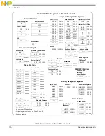
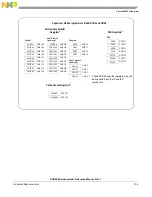
Table 13-1. L1CSR0 Field Descriptions (continued)
Field
Description
Summary of Contents for PXR4030
Page 1: ...PXR40 Microcontroller Reference Manual Devices Supported PXR4030 PXR4040 PXR40RM Rev 1 06 2011...
Page 30: ...PXR40 Microcontroller Reference Manual Rev 1 Freescale Semiconductor xxx...
Page 40: ...PXR40 Microcontroller Reference Manual Rev 1 xl Freescale Semiconductor...
Page 66: ...Memory Map PXR40 Microcontroller Reference Manual Rev 1 2 4 Freescale Semiconductor...
Page 120: ...Signal Descriptions 3 54 Freescale Semiconductor PXR40 Microcontroller Reference Manual Rev 1...
Page 860: ...FlexCAN Module 24 50 Freescale Semiconductor PXR40 Microcontroller Reference Manual Rev 1...
Page 1167: ...Decimation Filter Freescale Semiconductor 28 53 PXR40 Microcontroller Reference Manual Rev 1...
Page 1168: ...Decimation Filter 28 54 Freescale Semiconductor PXR40 Microcontroller Reference Manual Rev 1...


