


External Bus Interface (EBI)
Freescale Semiconductor
30-19
PXR40 Microcontroller Reference Manual, Rev. 1
real-time period is multiplied (by 2, 3, etc.) when a slower-speed mode is used, even though the BMT field
itself is unchanged.
30.4.1.7
Port Size Configuration per Chip Select (16 or 32 bits)
The EBI supports memories with data widths of 16 or 32 bits. The port size for a particular chip select is
configured by writing the PS bit in the corresponding Base Register.
30.4.1.8
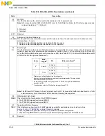
Configurable Wait States
From 0 to 15 wait states can be programmed for any cycle that the memory controller generates, via the
SCY bits in the appropriate Option Register. From 0 to 3 wait states between burst beats can be
programmed using the BSCY bits in the appropriate Option Register.
30.4.1.9
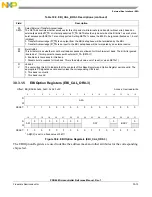
Configurable internal or external D_TA per chip select
Each chip select can be configured (via the SETA bit) to have D_TA driven internally (by the EBI), or
externally (by an external device). See
Section 30.3.1.4, EBI Base Registers (EBI_CAL_BR0-3)
, for more
details on SETA bit usage.
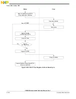
30.4.1.10 Support for Dynamic Calibration with up to 4 chip-selects
The EBI contains 4 calibration chip select signals, controlling 4 independent memory banks on the external
calibration bus. See
Section 30.4.2.10, Calibration Bus Operation
, for more details on using the calibration
bus.
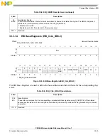
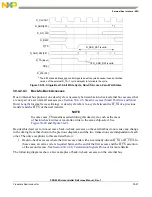
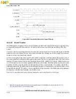
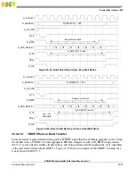
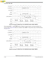
30.4.1.11 Four Write/Byte Enable (D_WE) Signals
The functionality of the D_WE[0:3] signals depends on the value of the WEBS bit in the corresponding
Base Register. Setting WEBS to 1 configures these pins as BE[0:3], while resetting it to 0 configures them
as WE[0:3]. WE[0:3] are asserted only during write accesses, while BE[0:3] is asserted for both read and
write accesses. The timing of the D_WE[0:3] signals remains the same in either case.
The upper Write/Byte Enable (D_WE0) indicates that the upper eight bits of the data bus
(D_ADD_DAT[0:7]) contain valid data during a write/read cycle. The upper middle Write/Byte Enable
(D_WE1) indicates that the upper middle eight bits of the data bus (D_ADD_DAT[8:15]) contain valid
data during a write/read cycle. The lower middle Write/Byte Enable (D_WE2) indicates that the lower
middle eight bits of the data bus (D_ADD_DAT[16:23]) contain valid data during a write/read cycle. The
lower Write/Byte Enable (D_WE3) indicates that the lower eight bits of the data bus
(D_ADD_DAT[24:31]) contain valid data during a write/read cycle.
Summary of Contents for PXR4030
Page 1: ...PXR40 Microcontroller Reference Manual Devices Supported PXR4030 PXR4040 PXR40RM Rev 1 06 2011...
Page 30: ...PXR40 Microcontroller Reference Manual Rev 1 Freescale Semiconductor xxx...
Page 40: ...PXR40 Microcontroller Reference Manual Rev 1 xl Freescale Semiconductor...
Page 66: ...Memory Map PXR40 Microcontroller Reference Manual Rev 1 2 4 Freescale Semiconductor...
Page 120: ...Signal Descriptions 3 54 Freescale Semiconductor PXR40 Microcontroller Reference Manual Rev 1...
Page 860: ...FlexCAN Module 24 50 Freescale Semiconductor PXR40 Microcontroller Reference Manual Rev 1...
Page 1167: ...Decimation Filter Freescale Semiconductor 28 53 PXR40 Microcontroller Reference Manual Rev 1...
Page 1168: ...Decimation Filter 28 54 Freescale Semiconductor PXR40 Microcontroller Reference Manual Rev 1...


