


Enhanced Direct Memory Access Controller (eDMA)
21-14
Freescale Semiconductor
PXR40 Microcontroller Reference Manual, Rev. 1
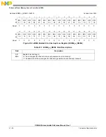
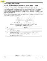
assigned by the channel priority registers. See
Section 21.3.2.17, eDMA Channel n Priority Registers
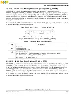
In round-robin arbitration mode, the channel priorities are ignored and the channels
within each group are cycled through, from channel 15 down to channel 0,without regard to priority.
The group priorities operate in a similar fashion. In group fixed-priority arbitration mode, channel service
requests in the highest priority group are executed first where priority level 3 (eDMA_A) or 1 (eDMA_B)
is the highest and priority level 0 is the lowest. The group priorities are assigned in the GRP
n
PRI fields of
the eDMA control register (EDMA_
x
_MCR). All group priorities must have unique values prior to any
channel service requests occur, otherwise a configuration error is reported. In group round-robin mode, the
group priorities are ignored and the groups are cycled through, from group 3 (eDMA_A) or 1 (eDMA_B)
down to group 0, without regard to priority.
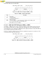
Minor loop offsets are address offset values added to the final source address (SADDR) or destination
address (DADDR) upon minor loop completion. When minor loop offsets are enabled, the minor loop
offset (MLOFF) is added to the final source address (SADDR) or to the final destination address
(DADDR) or to both addresses prior to the addresses being written back into the TCD. If the major loop
is complete, the minor loop offset is ignored and the major loop address offsets (SLAST and
DLAST_SGA) are used to compute the next EDMA
_x
_TCD.SADDR and EDMA
_x
_TCD.DADDR
values.
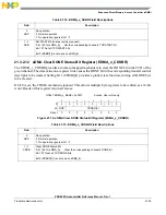
When minor loop mapping is enabled (EDMA_
x
_MCR[EMLM] = 1), TCD
n
word2 is redefined. A
portion of TCD
n
word2 is used to specify multiple fields: a source enable bit (SMLOE) to specify that the
minor loop offset should be applied to the source address (SADDR) upon minor loop completion, a
destination enable bit (DMLOE) to specify the minor loop offset should be applied to the destination
address (DADDR) upon minor loop completion, and the sign extended minor loop offset value (MLOFF).
The same offset value (MLOFF) is used for both source and destination minor loop offsets.
When either of the minor loop offsets is enabled (SMLOE is set or DMLOE is set), the NBYTES field is
reduced to 10 bits. When both minor loop offsets are disabled (SMLOE is cleared and DMLOE is cleared),
the NBYTES field becomes a 30-bit vector.
When minor loop mapping is disabled (EDMA_
x
_MCR[EMLM] = 0), all 32 bits of TCD
n
word2 are
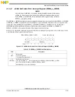
assigned to the NBYTES field. See
Section 21.3.2.18, Transfer Control Descriptor (TCD),
for more
details.
Summary of Contents for PXR4030
Page 1: ...PXR40 Microcontroller Reference Manual Devices Supported PXR4030 PXR4040 PXR40RM Rev 1 06 2011...
Page 30: ...PXR40 Microcontroller Reference Manual Rev 1 Freescale Semiconductor xxx...
Page 40: ...PXR40 Microcontroller Reference Manual Rev 1 xl Freescale Semiconductor...
Page 66: ...Memory Map PXR40 Microcontroller Reference Manual Rev 1 2 4 Freescale Semiconductor...
Page 120: ...Signal Descriptions 3 54 Freescale Semiconductor PXR40 Microcontroller Reference Manual Rev 1...
Page 860: ...FlexCAN Module 24 50 Freescale Semiconductor PXR40 Microcontroller Reference Manual Rev 1...
Page 1167: ...Decimation Filter Freescale Semiconductor 28 53 PXR40 Microcontroller Reference Manual Rev 1...
Page 1168: ...Decimation Filter 28 54 Freescale Semiconductor PXR40 Microcontroller Reference Manual Rev 1...


