


Enhanced Queued Analog-to-Digital Converter (EQADC)
27-58
Freescale Semiconductor
PXR40 Microcontroller Reference Manual, Rev. 1
2
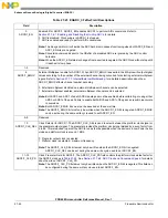
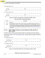
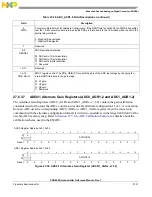
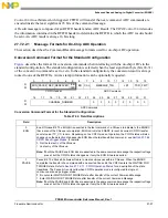
REP
Repeat/loop Start Point Indication Bit. The REP bit is asserted in the command to indicate where is the
start point of the sub-queue to be repeated when the streaming mode is enabled. The PAUSE bit indicates
the end point of the sub-queue. Therefore, both can occur in the same command or in separated ones. If
two or more REP bits are read before a PAUSE bit, this is an error case and the intermediary REP bits are
ignored.
0 It is not the start point of a loop.
1 Indicates the start point of the sub-queue to be repeated.
3–4
Reserved
5
EB
External Buffer Bit. A negated EB bit indicates that the command is sent to an internal CBuffer.
0 Command is sent to an internal buffer.
1 Reserved.
6
BN
Buffer Number Bit. BN indicates which buffer the message will be stored in.
1 Message stored in buffer 1.
0 Message stored in buffer 0.
7
CAL
Calibration Bit. CAL indicates if the returning conversion result must be calibrated.
1 Calibrate conversion result.
0 Do not calibrate conversion result.
8–11
MESSAGE_TAG
MESSAGE_TAG Field. The MESSAGE_TAG allows the EQADC to separate returning results into
different RFIFOs. When the EQADC transfers a command, the MESSAGE_TAG is included as part of the
command. Eventually the on-chip ADC returns the result with the same MESSAGE_TAG. The EQADC
separates incoming messages into different RFIFOs by decoding the MESSAGE_TAG of the incoming
data.
0000 Result is sent to RFIFO 0
0001 Result is sent to RFIFO 1
0010 Result is sent to RFIFO 2
0011 Result is sent to RFIFO 3
0100 Result is sent to RFIFO 4
0101 Result is sent to RFIFO 5
0110–0111 Reserved
1000 Null Message Received
1001 Reserved for customer use (see note)
1010 Reserved for customer use (see note)
1011–1111 Reserved
Note: These messages are treated as null messages.
12–13
LST
Long Sampling Time. These two bits determine the duration of the sampling time in ADC clock cycles.
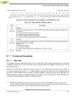
Table 27-32. Field Descriptions (continued)
Field
Description
LST[0:1]
Sampling cycles
(ADC Clock Cycles)
0b00
2
0b01
8
0b10
64
0b11
128
Summary of Contents for PXR4030
Page 1: ...PXR40 Microcontroller Reference Manual Devices Supported PXR4030 PXR4040 PXR40RM Rev 1 06 2011...
Page 30: ...PXR40 Microcontroller Reference Manual Rev 1 Freescale Semiconductor xxx...
Page 40: ...PXR40 Microcontroller Reference Manual Rev 1 xl Freescale Semiconductor...
Page 66: ...Memory Map PXR40 Microcontroller Reference Manual Rev 1 2 4 Freescale Semiconductor...
Page 120: ...Signal Descriptions 3 54 Freescale Semiconductor PXR40 Microcontroller Reference Manual Rev 1...
Page 860: ...FlexCAN Module 24 50 Freescale Semiconductor PXR40 Microcontroller Reference Manual Rev 1...
Page 1167: ...Decimation Filter Freescale Semiconductor 28 53 PXR40 Microcontroller Reference Manual Rev 1...
Page 1168: ...Decimation Filter 28 54 Freescale Semiconductor PXR40 Microcontroller Reference Manual Rev 1...


