
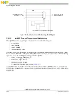


Boot Assist Module (BAM)
Freescale Semiconductor
9-7
PXR40 Microcontroller Reference Manual, Rev. 1
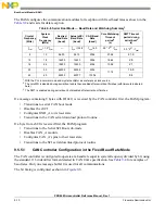
When enabled by RCHW[SWT, WTE] bits, the watchdog timeout periods are as shown in the
.
Note the following:
•
The core WD timeout for 20 and 40 MHz crystal is the same because the PLLCFG[2] pin should
be set for 40 MHz crystal, which has the effect of doubling the PLL input divider.
•
The SWT clock source is directly from the crystal oscillator. The core WD is clocked by the PLL.
•
The core WD timeouts reported here correspond to the PLL settings after reset. Core WD timeouts
will change as soon as the PLL is programmed with different multipliers.
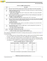
Table 9-4. RCHW Field Descriptions
Field
Description
0–3
Reserved. These bit values are ignored when the halfword is read. Program to 0 for future compatibility.
4
SWT
Software watchdog timer enable. This bit determines if the software watchdog timer is enabled after passing
control to the user application code.
0 Disable software watchdog timer
1 Enable software watchdog timer after reset. The timeout period is 392400 clock cycles (the default SWT
clock is the crystal oscillator).
5
WTE
MCU core watchdog timer enable. This bit determines if the core software watchdog timer is enabled.after
passing control to the user application code.
0 Disable core software watchdog timer
1 Enable core watchdog timer after reset. The timeout period is 2.5*2
17
system clocks.
6
PS0
Port size. Defines the width of the data bus connected to the memory on D_CS0. After system reset, the BAM
changes D_CS0 to a 16-bit port to fetch the RCHW from either 16- or 32-bit external memories. Then the BAM
reconfigures the EBI as a 16- or 32-bit port, depending on this bit.
0 32-bit D_CS0 port size
1 16-bit D_CS0 port size
Note: Used in development bus boot modes only (not available on all packages). Do not clear this bit if the
device only has a 16-bit data bus.
7
VLE
VLE Code Indicator. This bit configures the MMU entries 1-3 coded as Classic Book E instructions or as
Freescale VLE instructions.
0 User code executes as classic Book E code
1 User code executes as Freescale VLE code
8–15
BOOTID
Boot identifier. This field serves two functions:
• Indicates which block in flash memory contains the boot program
• Indicates if the flash memory is programmed (BOOTID=0x5A) or invalid
Table 9-5. Watchdog Timeout vs. Crystal Frequency
1
1
With the PLL in normal mode and crystal oscillator as a reference clock source.
Crystal Frequency (MHz)
Core WD Timeout (ms)
SWT Timeout (ms)
8
27.3
49
12
18.3
32.7
16
13.7
24.5
20
11
19.6
40
9.8
Summary of Contents for PXR4030
Page 1: ...PXR40 Microcontroller Reference Manual Devices Supported PXR4030 PXR4040 PXR40RM Rev 1 06 2011...
Page 30: ...PXR40 Microcontroller Reference Manual Rev 1 Freescale Semiconductor xxx...
Page 40: ...PXR40 Microcontroller Reference Manual Rev 1 xl Freescale Semiconductor...
Page 66: ...Memory Map PXR40 Microcontroller Reference Manual Rev 1 2 4 Freescale Semiconductor...
Page 120: ...Signal Descriptions 3 54 Freescale Semiconductor PXR40 Microcontroller Reference Manual Rev 1...
Page 860: ...FlexCAN Module 24 50 Freescale Semiconductor PXR40 Microcontroller Reference Manual Rev 1...
Page 1167: ...Decimation Filter Freescale Semiconductor 28 53 PXR40 Microcontroller Reference Manual Rev 1...
Page 1168: ...Decimation Filter 28 54 Freescale Semiconductor PXR40 Microcontroller Reference Manual Rev 1...


