


Signal Descriptions
3-52
Freescale Semiconductor
PXR40 Microcontroller Reference Manual, Rev. 1
3.3.11
JTAG and Nexus Signals
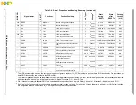
XTAL
XTAL is the output pin for an external crystal oscillator.
EXTAL
EXTAL is the input pin for an external crystal oscillator or an external clock source.
D_CLKOUT
CLKOUT is the device system clock output (for the development EBI).
ENGCLK
ENGCLK is a 50% duty cycle output clock with a maximum frequency of the device system
clock divided by two. ENGCLK is not synchronous to CLKOUT.
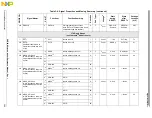
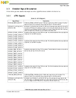
Table 3-15. JTAG and Nexus Signals
Signal Name
Description
EVTI
EVTI is an input that is read during a debug port reset to enable or disable the Nexus
Auxiliary port for data trace. After reset, the EVTI pin is used to initiate program and data
trace synchronization messages or generate a breakpoint.
EVTO
EVTO is an output that provides timing to a development tool for a single watchpoint or
breakpoint occurrence. The BAM uses this pin to select if auto baud rate is on or off
(
Section 9.3.4, Serial Boot Mode
MCKO
MCKO is a free running clock output to the development tools which is used for timing of
the MDO and MSEO signals.
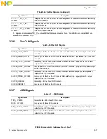
MDO0_GPIO220
1
1
GPIO function for MDO[11:0] is only available on Rev.2 of the device. Do not connect pin directly to a power supply or
ground.
MDO[0] is a trace message output to the development tools. In addition, MDO[0] indicates
the lock status of the system clock following a power-on reset. There is an internal pullup
on MDO[0]. This pin functions as GPIO when Nexus messaging is disabled.
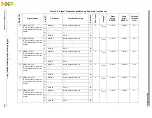
MDO[3:1]_GPIO[223:221]
MDO[3:1] are the trace message outputs to the development tools for reduced port mode.
These pins function as GPIO when Nexus messaging is disabled.
MDO[11:4]_GPIO[82:75]
MDO[11:4] are the trace message outputs to the development tools for reduced port
mode. These pins function as GPIO when Nexus messaging is disabled
MDO[15:12]_GPIO[234:231]
Trace message outputs to the development tools for full port mode. These pins function
as GPIO when the Nexus Development Interface (NDI) functions in reduced port mode or
when Nexus messaging is disabled
MSEO[1:0]
MSEO[1:0] are output signals that indicate when messages start and end on the MDO
pins.
RDY
RDY is an output signal that indicates to the development tools the data is ready to be read
from or written to the Nexus read/write access registers.
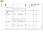
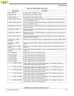
TCK
TCK provides the clock input for the on-chip test logic.
TDI
TDI provides the serial test instruction and data input for the on-chip test logic.
TDO
TDO provides the serial test data output for the on-chip test logic.
TMS
TMS controls test mode operations for the on-chip test logic.
JCOMP
JCOMP enables the JTAG TAP controller.
TEST
TEST places the chip into test mode. You must tie this pin to VSS.
Table 3-14. Reset and Clock Signals (continued)
Signal Name
Description
Summary of Contents for PXR4030
Page 1: ...PXR40 Microcontroller Reference Manual Devices Supported PXR4030 PXR4040 PXR40RM Rev 1 06 2011...
Page 30: ...PXR40 Microcontroller Reference Manual Rev 1 Freescale Semiconductor xxx...
Page 40: ...PXR40 Microcontroller Reference Manual Rev 1 xl Freescale Semiconductor...
Page 66: ...Memory Map PXR40 Microcontroller Reference Manual Rev 1 2 4 Freescale Semiconductor...
Page 120: ...Signal Descriptions 3 54 Freescale Semiconductor PXR40 Microcontroller Reference Manual Rev 1...
Page 860: ...FlexCAN Module 24 50 Freescale Semiconductor PXR40 Microcontroller Reference Manual Rev 1...
Page 1167: ...Decimation Filter Freescale Semiconductor 28 53 PXR40 Microcontroller Reference Manual Rev 1...
Page 1168: ...Decimation Filter 28 54 Freescale Semiconductor PXR40 Microcontroller Reference Manual Rev 1...


