


Enhanced Queued Analog-to-Digital Converter (EQADC)
27-64
Freescale Semiconductor
PXR40 Microcontroller Reference Manual, Rev. 1
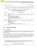
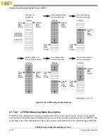
ADC Result Format for On-Chip ADC Operation
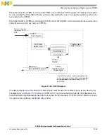
When the
FIFO Control Unit
receives a return data message, it decodes the MESSAGE_TAG field and
stores the 16-bit data into the appropriate RFIFO. This section describes the
ADC result
portion of the
result message
returned by the on-chip ADCs. The 16-bit data stored in the RFIFOs can be:
•
Data read from an ADC register with a read configuration command. In this case, the stored 16-bit
data corresponds to the contents of the ADC register that was read.
•
A time stamp. In this case, the stored 16-bit data is the value of the time base counter latched when
the EQADC detects the end of the analog input voltage sampling. For details see
•
A conversion result, coming directly from the ADCs. In this case, the stored 16-bit data contains a
right justified 14-bit result data. The conversion result can be calibrated or not depending on the
status of CAL bit in the command that requested the conversion
1
. When the CAL bit is negated,
this 14-bit data is obtained by executing a 2-bit left-shift on the 12-bit data resultant from the
resolution adjustment on the 8 or 10 or 12-bit data received from the ADC. The resolution
adjustment consists of changing the conversion result input from 8, 10 or 12 bits right aligned to a
12-bit word left aligned - refer to
Section 27.7.6.5, ADC Resolution Selection Feature
, for details.
When the CAL bit is asserted, this 14-bit data is the result of the calculations performed in the
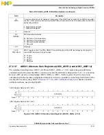
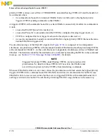
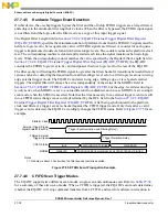
Table 27-35. Field Descriptions
Field
Description
0
EOQ
End Of Queue Bit
1
PAUSE
Pause Bit
2
REP
Repeat/loop Start Point Indication Bit
3–4
Reserved
5
EB
Must be 0b0
6
BN
Buffer Number Bit. Refer to
Section , Conversion Command Format for the Standard Configuration.
7
R/W
Read/Write bit. An asserted R/W bit indicates a read configuration command.
0 Write1Read
8–11
MESSAGE_
TAG
MESSAGE_TAG Field. Refer to
Section , Conversion Command Format for the Standard Configuration
.
12–23
Reserved
24–31
ADC_REG_
ADDRESS
ADC Register Address. The ADC_REG_ADDRESS field selects a register on the ADC register set to be
written or read. Only half-word addresses can be used.
1.
In case the conversion result is routed through an on-chip DSP via side interface, the calibration is applied before the data
is sent to the DSP.
Summary of Contents for PXR4030
Page 1: ...PXR40 Microcontroller Reference Manual Devices Supported PXR4030 PXR4040 PXR40RM Rev 1 06 2011...
Page 30: ...PXR40 Microcontroller Reference Manual Rev 1 Freescale Semiconductor xxx...
Page 40: ...PXR40 Microcontroller Reference Manual Rev 1 xl Freescale Semiconductor...
Page 66: ...Memory Map PXR40 Microcontroller Reference Manual Rev 1 2 4 Freescale Semiconductor...
Page 120: ...Signal Descriptions 3 54 Freescale Semiconductor PXR40 Microcontroller Reference Manual Rev 1...
Page 860: ...FlexCAN Module 24 50 Freescale Semiconductor PXR40 Microcontroller Reference Manual Rev 1...
Page 1167: ...Decimation Filter Freescale Semiconductor 28 53 PXR40 Microcontroller Reference Manual Rev 1...
Page 1168: ...Decimation Filter 28 54 Freescale Semiconductor PXR40 Microcontroller Reference Manual Rev 1...


