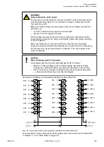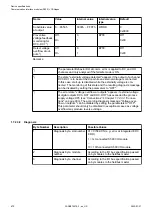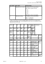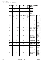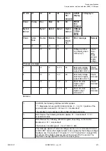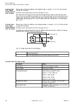
Table 143: Assignment of the other terminals
Terminal
Signal
Description
2.0
DC0
Signal of the configurable digital input/output DC0
2.1
DC1
Signal of the configurable digital input/output DC1
2.2
DC2
Signal of the configurable digital input/output DC2
2.3
DC3
Signal of the configurable digital input/output DC3
2.4
DC4
Signal of the configurable digital input/output DC4
2.5
DC5
Signal of the configurable digital input/output DC5
2.6
DC6
Signal of the configurable digital input/output DC6
2.7
DC7
Signal of the configurable digital input/output DC7
2.8
UP
Process voltage UP (24 V DC)
2.9
ZP
Process voltage ZP (0 V DC)
3.0
DI8
Signal of the digital input DI8
3.1
DI9
Signal of the digital input DI9
3.2
DI10
Signal of the digital input DI10
3.3
DI11
Signal of the digital input DI11
3.4
DI12
Signal of the digital input DI12
3.5
DI13
Signal of the digital input DI13
3.6
DI14
Signal of the digital input DI14
3.7
DI15
Signal of the digital input DI15
3.8
UP
Process voltage UP (24 V DC)
3.9
ZP
Process voltage ZP (0 V DC)
4.0
DO8
Signal of the digital output DO8
4.1
DO9
Signal of the digital output DO9
4.2
DO10
Signal of the digital output DO10
4.3
DO11
Signal of the digital output DO11
4.4
DO12
Signal of the digital output DO12
4.5
DO13
Signal of the digital output DO13
4.6
DO14
Signal of the digital output DO14
4.7
DO15
Signal of the digital output DO15
4.8
UP3
Process voltage UP3 (24 V DC)
4.9
ZP
Process voltage ZP (0 V DC)
Device specifications
Communication interface modules (S500) > CANopen
2022/01/31
3ADR010278, 3, en_US
664


