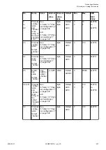


Terminal
Signal
Description
2.3
DI11
Signal of the digital input DI11
2.4
DI12
Signal of the digital input DI12
2.5
DI13
Signal of the digital input DI13
2.6
DI14
Signal of the digital input DI14
2.7
DI15
Signal of the digital input DI15
2.8
UP
Process voltage UP (24 V DC)
2.9
ZP
Process voltage ZP (0 V DC)
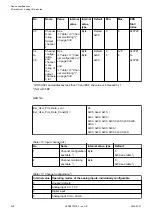
3.0
AI0+
Positive pole of analog input signal 0
3.1
AI1+
Positive pole of analog input signal 1
3.2
AI2+
Positive pole of analog input signal 2
3.3
AI3+
Positive pole of analog input signal 3
3.4
AI-
Negative pole of analog input signals 0 to 3
3.5
AO0+
Positive pole of analog output signal 0
3.6
AO1+
Positive pole of analog output signal 1
3.7
AO-
Negative pole of analog output signals 0
and 1
3.8
UP
Process voltage UP (24 V DC)
3.9
ZP
Process voltage ZP (0 V DC)
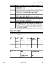
4.0
C16
Signal of the configurable digital input/
output C16
4.1
C17
Signal of the configurable digital input/
output C17
4.2
C18
Signal of the configurable digital input/
output C18
4.3
C19
Signal of the configurable digital input/
output C19
4.4
C20
Signal of the configurable digital input/
output C20
4.5
C21
Signal of the configurable digital input/
output C21
4.6
C22
Signal of the configurable digital input/
output C22
4.7
C23
Signal of the configurable digital input/
output C23
4.8
UP
Process voltage UP (24 V DC)
4.9
ZP
Process voltage ZP (0 V DC)
The internal power supply voltage for the module's circuitry is carried out via the I/O bus
(provided by a communication interface module or a CPU). Thus, the current consumption from
24 V DC power supply at the terminals L+/UP and M/ZP of the CPU/communication interface
module increases by 2 mA per DA501.
The external power supply connection is carried out via the UP (+24 V DC) and the ZP (0 V DC)
terminals.
Device specifications
I/O modules > Digital/Analog I/O modules
2022/01/31
3ADR010278, 3, en_US
551