


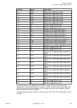

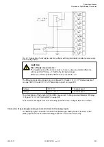

Parameter
Value
Conversion error of the analog values caused
by non-linearity, adjustment error at factory and
resolution within the normal range
Typ. 0.5 %, max. 1 %
For XC version below 0 °C and above 60 °C:
on request
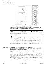
Relationship between input signal and hex code
Chapter 1.6.3.1.1.9.1 “Input ranges
voltage, current and digital input”
Chapter 1.6.3.1.1.9.2 “Input ranges resist-
ance temperature detector” on page 573
Unused inputs
Are configured as "unused" (default value)
Overvoltage protection
Yes
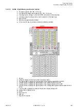
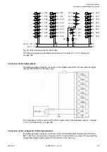
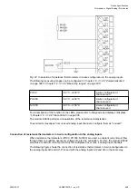
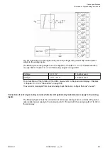
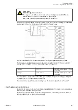
Technical data of the analog inputs, if used as digital inputs
Parameter
Value
Number of channels per module
Max. 4
Distribution of channels into groups
1 group of 4 channels
Connections of the channels AI0+ to AI3+
Terminals 3.0 to 3.3
Reference potential for the inputs
Terminals 1.9, 2.9, 3.9 and 4.9 (ZP)
Indication of the input signals
1 LED per channel
Input signal voltage
24 V DC
Signal 0
-30 V...+5 V
Undefined signal
+5 V...+13 V
Signal 1
+13 V...+30 V
Input current per channel
Input v24 V
Typ. 7 mA
Input v5 V
Typ. 1.4 mA
Input v15 V
Typ. 3.7 mA
Input v30 V
< 9 mA
Input resistance
ca. 3.5 k
W
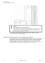
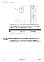
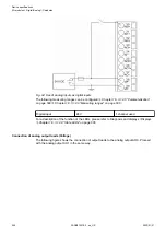
Technical data of the analog outputs
Parameter
Value
Number of channels per module
2
Distribution of channels into groups
1 group for 2 channels
Connection of the channels AO0+...AO1+
Terminals 3.5 and 3.6
Reference potential for AO0+ to AO1+
Terminal 3.7 (AO-) for voltage output
Terminals 1.9, 2.9, 3.9 and 4.9 for current
output
Output type
Unipolar
Current
Bipolar
Voltage
Device specifications
I/O modules > Digital/Analog I/O modules
2022/01/31
3ADR010278, 3, en_US
581