285
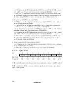
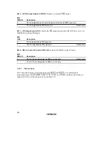
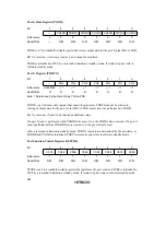
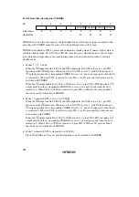
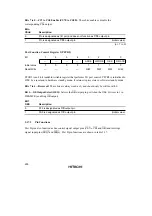
Bits 7 to 0—CS7 to CS0 Enable (CS7E to CS0E): These bits enable or disable the
corresponding
CSn
output.
Bit n
CSnE
Description
0
Pin is designated as I/O port and does not function as
CSn
output pin
1
Pin is designated as
CSn
output pin
(Initial value)
(n = 7 to 0)
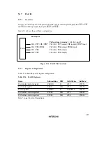
5.16.3
Pin Functions
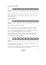
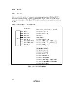
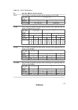
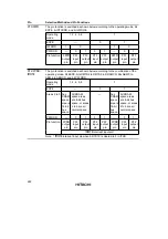
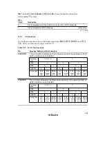
Port G pins also function as bus control signal output pins (
BREQ
,
BACK,
BREQO
, and
CS3
to
CS0
). Port G pin functions are shown in table 5.35.
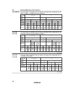
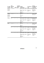
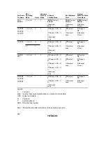
Table 5.35
Port G Pin Functions
Pin
Selection Method and Pin Functions
PG6/
BREQ
The pin function is switched as shown below according to the operating mode, bit
EXPE, bit BRLE, and bit PG6DDR.
Operating
mode
1, 2, 4, 5, 6
7
EXPE
—
0
1
BRLE
0
1
—
0
1
PG6DDR
0
1
—
0
1
0
1
—
Pin function
PG6
input
pin
PG6
output
pin
BREQ
input
pin
PG6
input
pin
PG6
output
pin
PG6
input
pin
PG6
output
pin
BREQ
input
pin
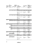
PG5/
BACK
The pin function is switched as shown below according to the operating mode, bit
EXPE, bit BRLE, and bit PG5DDR.
Operating
mode
1, 2, 4, 5, 6
7
EXPE
—
0
1
BRLE
0
1
—
0
1
PG5DDR
0
1
—
0
1
0
1
—
Pin function
PG5
input
pin
PG5
output
pin
BACK
output
pin
PG5
input
pin
PG5
output
pin
PG5
input
pin
PG5
output
pin
BACK
output
pin
Содержание H8S/2670
Страница 5: ......
Страница 9: ......
Страница 199: ...182 ...
Страница 361: ...344 ...
Страница 393: ...376 ...
Страница 647: ...630 ...

