167
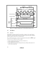
T
1
Address bus
ø
RD
Bus cycle A
T
2
T
3
T
1
T
2
Bus cycle B
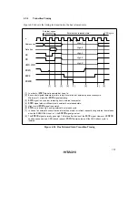
Possibility of overlap between
CS
(area B) and
RD
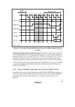
(a) Idle cycle not inserted
(ICIS1 = 0)
T
1
Address bus
ø
Bus cycle A
T
2
T
3
T
i
T
1
Bus cycle B
(b) Idle cycle inserted
(ICIS1 = 1 (initial value))
T
2
CS
(area A)
CS
(area B)
RD
CS
(area A)
CS
(area B)
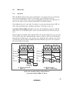
Figure 4.46 Relationship between Chip Select (
CS
) and Read (
RD
)
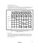
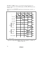
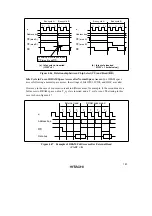
Idle Cycle in Case of DRAM Space Access after Normal Space Access: In a DRAM space
access following a normal space access, the settings of bits ICIS1, ICIS0, and IDLC are valid.
However, in the case of consecutive reads in different areas, for example, if the second read is a
full access to DRAM space, only a T
p
cycle is inserted, and a T
i
cycle is not. The timing in this
case is shown figure 4.47.
T
1
Address bus
ø
RD
External read
Data bus
T
2
T
3
T
p
T
r
DRAM space read
T
c1
T
c2
Figure 4.47 Example of DRAM Full Access after External Read
(CAST = 0)
Содержание H8S/2670
Страница 5: ......
Страница 9: ......
Страница 199: ...182 ...
Страница 361: ...344 ...
Страница 393: ...376 ...
Страница 647: ...630 ...

