174
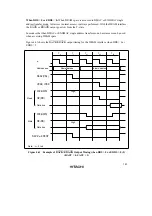
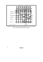
T
1
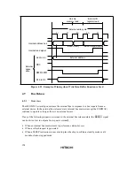
Internal address bus
A23 to A0
External write cycle
HWR
,
LWR
T
2
T
W
T
W
T
3
On-chip
memory read
Internal I/O
register read
Internal read signal
CSn
D15 to D0
External address
Internal memory
External
space
write
Internal I/O register address
Figure 4.53 Example of Timing when Write Data Buffer Function is Used
4.9
Bus Release
4.9.1
Overview
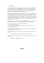
The H8S/2678 Series chip can release the external bus in response to a bus request from an
external device. In the external bus released state, internal bus masters (except the EXDMAC)
continue to operate as long as there is no external access.
If any of the following requests are issued in the external bus released state, the
BREQO
signal
can be driven low to output a bus request externally.
•
When an internal bus master wants to perform an external access
•
When a refresh request is generated
•
When a SLEEP instruction is executed to place the chip in software standby mode or all-
module-clocks-stopped mode
Содержание H8S/2670
Страница 5: ......
Страница 9: ......
Страница 199: ...182 ...
Страница 361: ...344 ...
Страница 393: ...376 ...
Страница 647: ...630 ...

