476
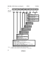
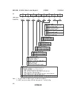
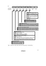
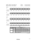
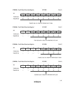
EDMDR2—EXDMA Mode Control Register 2
H'FDEC
EXDMAC
Bit
Initial value
Read/Write
15
EDA
0
R/(W)
*
1
14
BEF
0
R/(W)
*
2
13
EDRAKE
0
R/W
12
ETENDE
0
R/W
11
EDREQS
0
R/W
10
AMS
0
R/W
9
MDS1
0
R/W
8
MDS0
0
R/W
Address Mode Select
0
Dual address mode
1
Single address mode
EDREQ
Select
0
Low level sensing
1
Falling edge sensing
ETEND
Pin Output Enable
0
ETEND
pin output disabled
1
ETEND
pin output enabled
EDRAK
Pin Output Enable
0
EDRAK
pin output disabled
1
EDRAK
pin output enabled
Block Transfer Error Flag
0
No block transfer error
[Clearing condition]
Writing 0 to BEF after reading BEF = 1
1
Block transfer error
[Setting condition]
NMI interrupt during block transfer
EXDMA Active
0
Data transfer disabled on corresponding channel
[Clearing conditions]
• When the specified number of transfers end
• When operation is halted by a repeat area overflow interrupt
• When 0 is written to EDA while EDA = 1
(In block transfer mode, write is effective after end of one-block transfer)
• Reset, NMI interrupt, or hardware standby mode
1
Data transfer enabled on corresponding channel. EXDMA operation in progress
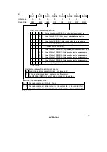
Mode Select 1 and 0
0
Auto request, cycle steal mode,
normal transfer mode
1
0
1
0
1
Auto request, burst mode,
normal transfer mode
External request, cycle steal mode,
normal transfer mode
External request, cycle steal mode,
block transfer mode
Notes: 1. The value written in bit EDA may not be effective immediately.
2. Bit BEF can only be written with 0 after being read as 1, to clear the flag.
Содержание H8S/2670
Страница 5: ......
Страница 9: ......
Страница 199: ...182 ...
Страница 361: ...344 ...
Страница 393: ...376 ...
Страница 647: ...630 ...


