142
output from both the
RD
pin and the
OE
pin, but in external read cycles for other than DRAM
space, the signal is output only from the
RD
pin.
4.5.7
Column Address Output Cycle Control
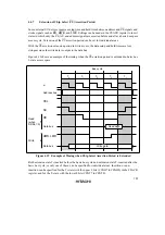
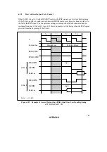
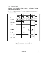
The column address output cycle can be changed from 2 states to 3 states by setting the CAST bit
to 1 in the DRAMCR register. Use the setting that gives the optimum specification values (
CAS
pulse width, etc.) according to the DRAM connected and the operating frequency of the chip.
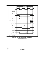
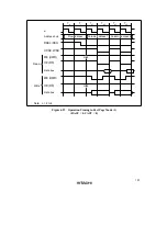
Figure 4.21 shows an example of the timing when a 3-state column address output cycle is
selected.
T
p
ø
RASn
(
CSn
)
Read
Write
UCAS
,
LCAS
WE
(
HWR
)
OE
(
RD
)
Data bus
WE
(
HWR
)
OE
(
RD
)
Data bus
Address bus
T
r
T
c1
T
c2
T
c3
Row address
Column address
High
High
Note: n = 2 to 5
Figure 4.21 Example of Access Timing with 3-State Column Address Output Cycle
(RAST = 0)
Содержание H8S/2670
Страница 5: ......
Страница 9: ......
Страница 199: ...182 ...
Страница 361: ...344 ...
Страница 393: ...376 ...
Страница 647: ...630 ...


