152
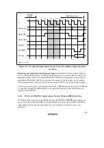
T
p
ø
T
r
T
c1
T
c2
T
c3
T
c1
T
c2
T
c3
RASn
(
CSn
)
Read
Write
UCAS
,
LCAS
WE
(
HWR
)
OE
(
RD
)
Data bus
WE
(
HWR
)
OE
(
RD
)
Data bus
Address bus
Note: n = 2 to 5
Row address
Column address 1
Column address 2
High
High
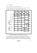
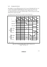
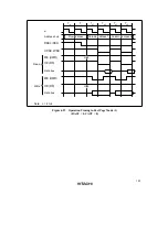
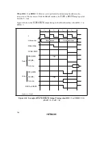
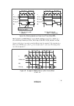
Figure 4.30 Operation Timing in Fast Page Mode (2)
(RAST = 0, CAST = 1)
The bus cycle can also be extended in burst access by inserting wait states. The wait state insertion
method and timing are the same as for full access. For details see section 4.5.10, Wait Control.
RAS Down Mode and RAS Up Mode: Even when burst operation is selected, it may happen that
access to DRAM space is not continuous, but is interrupted by access to another space. In this
case, if the
RAS
signal is held low during the access to the other space, burst operation can be
resumed when the same row address in DRAM space is accessed again.
•
RAS Down Mode
To select RAS down mode, set both the RCDM bit and the BE bit to 1 in DRAMCR. If access
to DRAM space is interrupted and another space is accessed, the
RAS
signal is held low during
the access to the other space, and burst access is performed when the row address of the next
DRAM space access is the same as the row address of the previous DRAM space access.
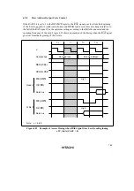
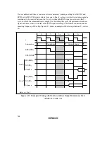
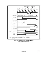
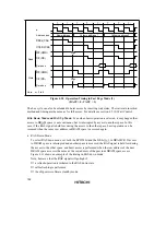
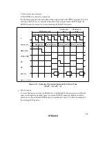
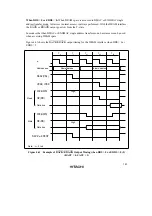
Figure 4.31 shows an example of the timing in RAS down mode.
Note, however, that the
RAS
signal will go high if:
a refresh operation is initiated in the RAS down state
self-refreshing is performed
the chip enters software standby mode
Содержание H8S/2670
Страница 5: ......
Страница 9: ......
Страница 199: ...182 ...
Страница 361: ...344 ...
Страница 393: ...376 ...
Страница 647: ...630 ...


