141
4.5.6
Basic Timing
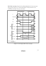
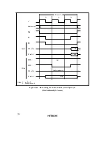
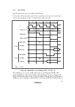
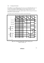
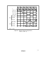
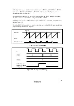
Figure 4.20 shows the basic access timing for DRAM space.
The four states of the basic timing consist of one T
p
(precharge cycle) state, one T
r
(row address
output cycle) state, and the T
c1
and T
c2
(column address output cycle) states.
T
p
ø
RASn
(
CSn
)
Read
Write
UCAS
,
LCAS
WE
(
HWR
)
OE
(
RD
)
Data bus
WE
(
HWR
)
OE
(
RD
)
Data bus
Address bus
T
r
T
c1
T
c2
Row address
High
High
Column address
Note: n = 2 to 5
Figure 4.20 DRAM Basic Access Timing (RAST = 0, CAST = 0)
When DRAM space is accessed, the
RD
signal is output as the
OE
signal for DRAM. When
connecting DRAM provided with an EDO page mode, the
OE
signal should be connected to the
OE
pin of the DRAM. Setting the OEE bit to 1 in the DRAMCR register enables the
OE
signal for
DRAM space to be output from a dedicated
OE
pin. In this case, the
OE
signal for DRAM space is
Содержание H8S/2670
Страница 5: ......
Страница 9: ......
Страница 199: ...182 ...
Страница 361: ...344 ...
Страница 393: ...376 ...
Страница 647: ...630 ...

