603
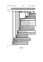
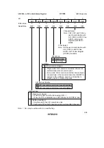
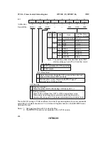
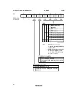
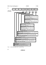
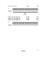
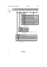
TCR0—Timer Control Register 0
H'FFB0
8-Bit Timer Channel 0
TCR1—Timer Control Register 1
H'FFB1
8-Bit Timer Channel 1
Bit
Initial value
Read/Write
7
CMIEB
0
R/W
6
CMIEA
0
R/W
5
OVIE
0
R/W
4
CCLR1
0
R/W
3
CCLR0
0
R/W
2
CKS2
0
R/W
1
CKS1
0
R/W
0
CKS0
0
R/W
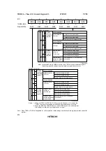
Clock Select
0
Clock input disabled
1
0
1
Internal clock: count at falling
edge of ø/8
Internal clock: count at falling
edge of ø/64
Internal clock: count at falling
edge of ø/8192
For channel 0:
Count at TCNT1 overflow signal
*
For channel 1:
Count at TCNT0 compare match A
External clock: count at rising edge
0
1
0
1
0
0
1
External clock: count at falling edge
1
0
External clock: count at both rising
and falling edges
1
Note:
*
If the clock input of channel 0 is the
TCNT1 overflow signal and that of
channel 1 is the TCNT0 compare match
signal, no incrementing clock is
generated. Do not use this setting.
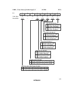
Counter Clear
0
Clearing is disabled
1
0
1
0
1
Clear by compare match A
Clear by compare match B
Clear by rising edge of external reset input
Timer Overflow Interrupt Enable
0
OVF interrupt request (OVI) is disabled
1
OVF interrupt request (OVI) is enabled
Compare Match Interrupt Enable A
0
CMFA interrupt request (CMIA) is disabled
1
CMFA interrupt request (CMIA) is enabled
Compare Match Interrupt Enable B
0
CMFB interrupt request (CMIB) is disabled
1
CMFB interrupt request (CMIB) is enabled
Содержание H8S/2670
Страница 5: ......
Страница 9: ......
Страница 199: ...182 ...
Страница 361: ...344 ...
Страница 393: ...376 ...
Страница 647: ...630 ...

