156
T
Rp
ø
CSn
(
RASn
)
T
Rr
T
Rc1
T
Rc2
UCAS
,
LCAS
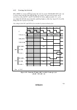
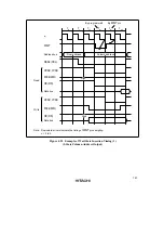
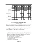
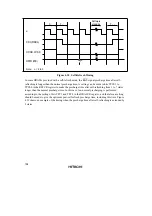
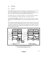
Figure 4.35 CBR Refresh Timing
A setting can be made in bits RCW1 and RCW0 to delay
RAS
signal output by one to three
cycles. Use bits RLW1 and RLW0 to adjust the width of the
RAS
signal. The settings of bits
RCW1, RCW0, RLW1, and RLW0 are valid only in refresh operations.
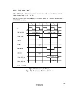
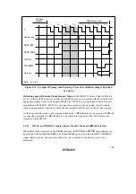
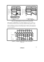
Figure 4.36 shows the timing when bits RCW1 and RCW0 are set to 0 and 1, respectively.
T
Rp
ø
CSn
(
RASn
)
T
Rrw
T
Rr
T
Rc1
UCAS
,
LCAS
T
Rc2
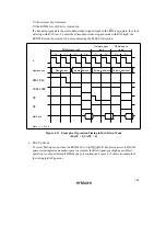
Figure 4.36 CBR Refresh Timing
(RCW1 = 0, RCW0 = 1, RLW1 = 0, RLW0 = 0)
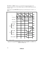
Depending on the DRAM used, modification of the
WE
signal may not be permitted during the
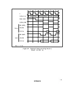
refresh period. In this case, the CBRM bit should be set to 1. The bus controller will then insert
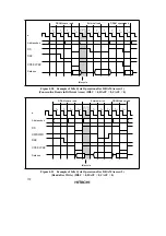
refresh cycles in appropriate breaks between bus cycles. Figure 4.37 shows an example of the
timing when the CBRM bit is set to 1. In this case the
CS
signal is not controlled, and retains its
value prior to the start of the refresh period.
Содержание H8S/2670
Страница 5: ......
Страница 9: ......
Страница 199: ...182 ...
Страница 361: ...344 ...
Страница 393: ...376 ...
Страница 647: ...630 ...


