456
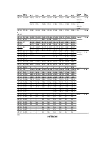
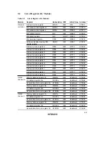
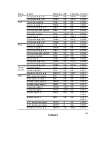
Module
Register
Abbreviation R/W
Initial Value Address
*
1
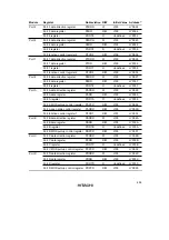
Port E
Port E data direction register
PEDDR
W
H'00
H'FE2D
Port E data register
PEDR
R/W
H'00
H'FF6D
Port E register
PORTE
R
Undefined
H'FF5D
Port E MOS pull-up control register
PEPCR
R/W
H'00
H'FE3A
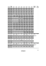
Port F
Port F data direction register
PFDDR
W
H'80/H'00
*
17
H'FE2E
Port F data register
PFDR
R/W
H'00
H'FF6E
Port F register
PORTF
R
Undefined
H'FF5E
Port function control register 2
PFCR2
R/W
H'0E
H'FE34
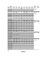
Port G
Port G data direction register
PGDDR
W
H'01/H'00
*
17
H'FE2F
Port G data register
PGDR
R/W
H'00
H'FF6F
Port G register
PORTG
R
Undefined
H'FF5F
Port function control register 0
PFCR0
R/W
H'FF
H'FE32
Port H
Port H data direction register
PHDDR
W
H'00
H'FF74
Port H data register
PHDR
R/W
H'00
H'FF72
Port H register
PORTH
R
Undefined
H'FF70
Port function control register 0
PFCR0
R/W
H'FF
H'FE32
Port function control register 2
PFCR2
R/W
H'0E
H'FE34
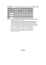
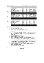
Notes: 1. Lower 16 bits of the address.
2. Only 0 can be written for flag clearing.
3. Registers in the DTC cannot be read or written to directly.
4. Located as register information in on-chip RAM addresses H'BC00 to H'BFFF. Cannot
be located in external memory space. Do not clear the RAME bit in SYSCR to 0 when
using the DTC.
5. The value written in bit 15 of EDMDR0 to EDMDR3 may not be effective immediately.
Bits 14 and 6 of EDMDR0 to EDMDR3 can only be written with 0 after being read as 1,
to clear the flags.
6. Determined by the MCU operating mode.
7. Bits used for pulse output cannot be written to.
8. If the pulse output group 2 and pulse output group 3 output triggers are the same
according to the PCR setting, the NDRH address will be H'FF4C, and if different, the
address of NDRH for group 2 will be H'FF4E, and that for group 3 will be H'FF4C.
Similarly, if the pulse output group 0 and pulse output group 1 output triggers are the
same according to the PCR setting, the NDRL address will be H'FF4D, and if different,
the address of NDRL for group 0 will be H'FF4F, and that for group 1 will be H'FF4D.
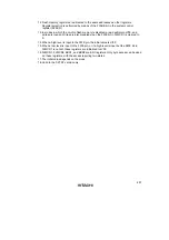
9. Only 0 can be written to bits 7 to 5, to clear the flags.
10. For information on writing, see section 11.2.4, Notes on Register Access, in the
H8S/2678 Series Hardware Manual.
11. Only 0 can be written to bit 7, to clear the flag.
Содержание H8S/2670
Страница 5: ......
Страница 9: ......
Страница 199: ...182 ...
Страница 361: ...344 ...
Страница 393: ...376 ...
Страница 647: ...630 ...

