620
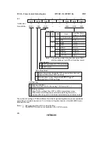
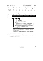
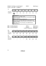
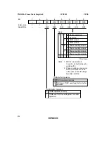
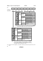
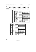
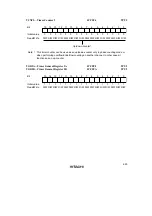
TIOR1—Timer I/O Control Register 1
H'FFE2
TPU1
Bit
Initial value
Read/Write
7
IOB3
0
R/W
6
IOB2
0
R/W
5
IOB1
0
R/W
4
IOB0
0
R/W
3
IOA3
0
R/W
2
IOA2
0
R/W
1
IOA1
0
R/W
0
IOA0
0
R/W
0
0
TGR1A I/O Control
0
0
1
TGR1A
is output
compare
register
1
0
1
1
0
0
1
1
0
1
0
1
0
0
TGR1A
is input
capture
register
1
1
*
Output disabled
Initial output is
1 output
Output disabled
Initial output is
0 output
Capture input
source is
TIOCA4 pin
0 output at compare match
1 output at compare match
Toggle output at compare match
*
: Don’t care
0 output at compare match
1 output at compare match
Toggle output at compare match
Input capture at rising edge
Input capture at falling edge
Input capture at both edges
*
*
1
Capture input
source is TGR0A
compare match/
input capture
Input capture at generation of
channel 0/TGR0A compare match/
input capture
0
0
TGR1B I/O Control
0
0
1
TGR1B
is output
compare
register
1
0
1
1
0
0
1
1
0
1
0
1
0
0
TGR1B
is input
capture
register
1
1
*
Output disabled
Initial output is
1 output
Output disabled
Initial output is
0 output
Capture input
source is
TIOCB1 pin
0 output at compare match
1 output at compare match
Toggle output at compare match
*
: Don’t care
0 output at compare match
1 output at compare match
Toggle output at compare match
Input capture at rising edge
Input capture at falling edge
Input capture at both edges
*
*
1
Capture input
source is TGR0C
compare match/
input capture
Input capture at generation of
TGR0C compare match/
input capture
Содержание H8S/2670
Страница 5: ......
Страница 9: ......
Страница 199: ...182 ...
Страница 361: ...344 ...
Страница 393: ...376 ...
Страница 647: ...630 ...

