219
Pin
Selection Method and Pin Functions
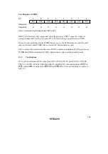
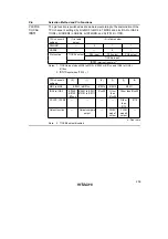
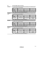
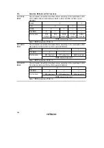
P33/RxD1
The pin function is switched as shown below according to the combination of bit
RE in SCR of SCI1 and bit P33DDR.
RE
0
1
P33DDR
0
1
—
Pin function
P33 input pin
P33 output pin
*
RxD1 input pin
Note:
*
NMOS open-drain output when P33ODR = 1.
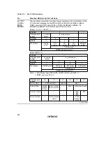
P32/RxD0/
IrRxD
The pin function is switched as shown below according to the combination of bit
RE in SCR of SCI0 and bit P32DDR.
RE
0
1
P32DDR
0
1
—
Pin function
P32 input pin
P32 output pin
*
RxD0/IrRxD
input pin
Note:
*
NMOS open-drain output when P32ODR = 1.
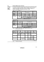
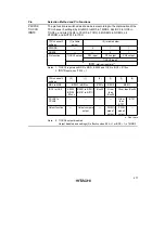
P31/TxD1
The pin function is switched as shown below according to the combination of bit
TE in SCR of SCI1 and bit P31DDR.
TE
0
1
P31DDR
0
1
—
Pin function
P31 input pin
P31 output pin
*
TxD1 output pin
*
Note:
*
NMOS open-drain output when P31ODR = 1.
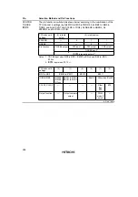
P30/TxD0/
IrTxD
The pin function is switched as shown below according to the combination of bit
TE in SCR of SCI0 and bit P30DDR.
TE
0
1
P30DDR
0
1
—
Pin function
P30 input pin
P30 output pin
*
TxD0/IrTxD
output pin
*
Note:
*
NMOS open-drain output when P30ODR = 1.
Содержание H8S/2670
Страница 5: ......
Страница 9: ......
Страница 199: ...182 ...
Страница 361: ...344 ...
Страница 393: ...376 ...
Страница 647: ...630 ...

