280
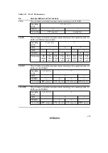
Pin
Selection Method and Pin Functions
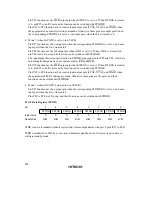
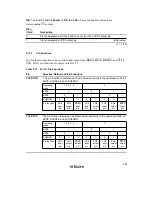
PF3/
LWR
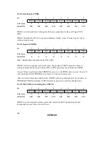
The pin function is switched as shown below according to the operating mode, bit
EXPE, bit PF3DDR, and bit LWROE.
Operating
mode
1, 2, 4, 5, 6
7
EXPE
—
0
1
LWROD
1
0
—
1
0
PF3DDR
—
0
1
0
1
—
0
1
Pin function
LWR
output
pin
PF3
input
pin
PF3
output
pin
PF3
input
pin
PF3
output
pin
LWR
output
pin
PF3
input
pin
PF3
output
pin
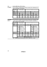
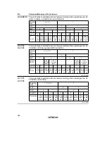
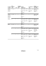
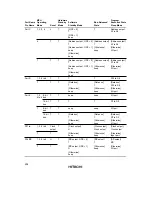
PF2/
LCAS
/
IRQ15
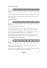
The pin function is switched as shown below according to the combination of the
operating mode, bit EXPE, bits RMTS2 to RMTS0 in DRAMCR, bits ABW5 to
ABW2 in ABWCR, and bit PF2DDR.
Operating
mode
1, 2, 4, 5, 6
7
EXPE
—
0
1
Areas 2 to 5 Any
DRAM
space
area is
16-bit
bus
space
All DRAM
space areas
are 8-bit bus
space, or areas
2 to 5 are all
normal space
—
Any
DRAM
space
area is
16-bit
bus
space
All DRAM
space areas
are 8-bit bus
space, or areas
2 to 5 are all
normal space
PF2DDR
—
0
1
0
1
—
0
1
Pin function
LCAS
output
pin
PF2
input
pin
PF2
output
pin
PF2
input
pin
PF2
output
pin
LCAS
output
pin
PF2
input
pin
PF2
output
pin
IRQ15
interrupt input pin
*
Note:
*
IRQ15
interrupt input pin when bit ITS15 is cleared to 0 in ITSR.
Содержание H8S/2670
Страница 5: ......
Страница 9: ......
Страница 199: ...182 ...
Страница 361: ...344 ...
Страница 393: ...376 ...
Страница 647: ...630 ...

