120
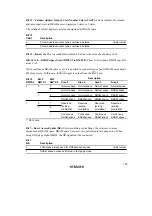
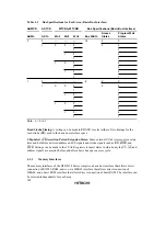
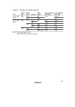
Table 4.3
Bus Specifications for Each Area (Basic Bus Interface)
ABWCR
ASTCR
WTCRA, WTCRB
Bus Specifications (Basic Bus Interface)
ABWn
ASTn
Wn2
Wn1
Wn0
Bus Width
Access
States
Program Wait
States
0
0
—
—
—
16
2
0
1
0
0
0
3
0
1
1
1
0
2
1
3
1
0
0
4
1
5
1
0
6
1
7
1
0
—
—
—
8
2
0
1
0
0
0
3
0
1
1
1
0
2
1
3
1
0
0
4
1
5
1
0
6
1
7
Note:
n = 0 to 7
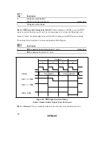
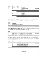
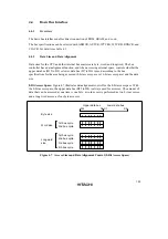
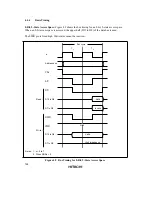
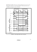
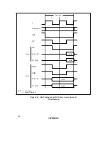
Read Strobe Timing: A setting can be made in RDNCR to select either of two timings for the
read strobe (
RD
) used in the basic bus interface space.
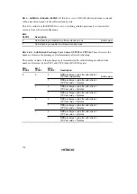
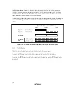
Chip Select (
CS
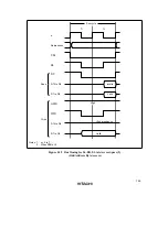
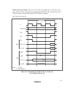
) Assertion Period Extension States: Some external I/O devices require a setup
time and hold time between address and
CS
signals and strobe signals such as
RD
,
HWR
, and
LWR
. Settings can be made in the CSACR registers to insert states in which only the
CS
,
AS
, and
address signals are asserted before and after a basic bus space access cycle.
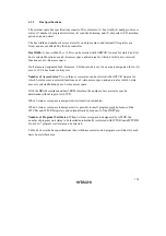
4.3.3
Memory Interfaces
The memory interfaces of the H8S/2678 Series comprise a basic bus interface that allows direct
connection of ROM, SRAM, and so on; a DRAM interface that allows direct connection of
DRAM; and a burst ROM interface that allows direct connection of burst ROM. The interface can
be selected independently for each area.
Содержание H8S/2670
Страница 5: ......
Страница 9: ......
Страница 199: ...182 ...
Страница 361: ...344 ...
Страница 393: ...376 ...
Страница 647: ...630 ...

