ISD94100 Series Technical Reference Manual
Sep 9, 2019
Page
818
of 928
Rev1.09
IS
D
9
410
0
S
ER
IE
S
T
E
C
HN
ICA
L
RE
F
E
RE
NCE
M
AN
U
AL
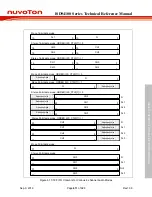
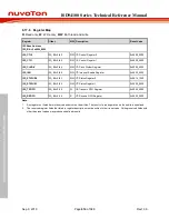
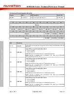
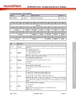
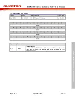
I2S Control Register 1 (I2S_CTL1)
Register
Offset
R/W Description
Reset Value
I2S_CTL1
0x20
R/W I
2
S Control Register 1
0x0000_0000
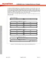
31
30
29
28
27
26
25
24
Reserved
PB16ORD
PBWIDTH
23
22
21
20
19
18
17
16
Reserved
RXTH
15
14
13
12
11
10
9
8
Reserved
TXTH
7
6
5
4
3
2
1
0
CH7ZCEN
CH6ZCEN
CH5ZCEN
CH4ZCEN
CH3ZCEN
CH2ZCEN
CH1ZCEN
CH0ZCEN
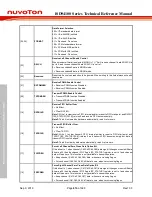
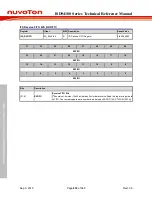
Bits
Description
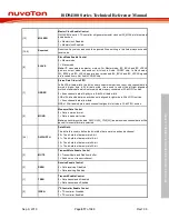
[31:26]
Reserved
Reserved. Any values read should be ignored. When writing to this field always write with
reset value.
[25]
PB16ORD
FIFO Read/Write Order in 16-bit Width of Peripheral Bus
When PBWIDTH = 1, the data FIFO will be increased or decreased by two peripheral bus
access. This bit is used to select the order of FIFO access operations to meet the 32-bit
transmitting/receiving FIFO entries.
0 = Low 16-bit read/write access first.
1 = High 16-bit read/write access first.
Note:
This bit is available while PBWIDTH = 1.
[24]
PBWIDTH
Peripheral Bus Data Width Selection
This bit is used to choice the available data width of APB bus. It must be set to 1 while PDMA
function is enable and it is set to 16-bit transmission mode
0 = 32 bits data width.
1 = 16 bits data width.
Note1:
If PBWIDTH=1, the low 16 bits of 32-bit data bus are available.
Note2:
If PBWIDTH=1, the transmitting FIFO level will be increased after two FIFO write
operations.
Note3:
If PBWIDTH=1, the receiving FIFO level will be decreased after two FIFO read
operations.
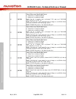
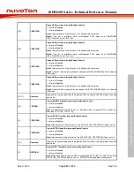
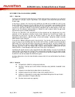
[23:20]
Reserved
Reserved. Any values read should be ignored. When writing to this field always write with
reset value.


