ISD94100 Series Technical Reference Manual
Sep 9, 2019
Page
677
of 928
Rev1.09
IS
D
9
410
0
S
ER
IE
S
T
E
C
HN
ICA
L
RE
F
E
RE
NCE
M
AN
U
AL
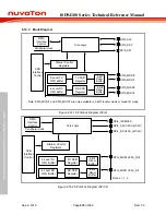
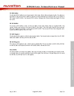
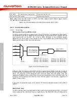
TX FIFO Buffer:
The transmit FIFO buffer is a 4-/8-level depth, 32-bit wide, first-in, first-out register buffer. The data can
be written to the transmit FIFO buffer in advance through software by writing the SPIn_TX register. In
SPI mode for SPI1~SPI2, The transmit FIFO will be configured as 8-level while data length is set as
8~16 bits.
RX FIFO Buffer:
The receive FIFO buffer is also a 4-/8-level depth, 32-bit wide, first-in, first-out register buffer. The
receive control logic will store the receive data to this buffer. The FIFO buffer data can be read from
SPIn_RX register by software. In SPI mode for SPI1~SPI2, The receive FIFO will be configured as 8-
level while data length is set as 8~16 bits.
TX Shift Register:
The transmit shift register is a 32-bit wide register buffer. The transmit data is loaded from the TX FIFO
buffer and shifted out bit-by-bit to the skew buffer.
RX Shift Register:
The receive shift register is also a 32-bit wide register buffer. The receive data is shift in bit-by-bit from
the skew buffer and is loaded into RX FIFO buffer when a transaction done.
Skew Buffer:
The skew buffer is a 4-level 1-bit buffer. There are two skew buffers in transmitting and received side.
In received side, it is used to shift bits into Rx shift register from SPI bus. In transmitting side, it is used
to shift bits into SPI bus from Tx shift register.


