ISD94100 Series Technical Reference Manual
Sep 9, 2019
Page
693
of 928
Rev1.09
IS
D
9
410
0
S
ER
IE
S
T
E
C
HN
ICA
L
RE
F
E
RE
NCE
M
AN
U
AL
Comparator
Valid Data Count in
Transmit FIFO Buffer
TXTHIF = 1 when A <= B
TXTHIF = 0 when A > B
TXTH
Comparator
Valid Data Count in
Receive FIFO Buffer
RXTH
A
B
C
D
RXTHIF = 1 when C > D
RXTHIF = 0 when C <= D
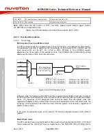
Figure 6.14-22 FIFO Threshold Comparator
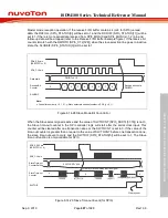
In Master mode, when the first datum is written to the SPIn_TX register, the TXEMPTY flag
(SPIn_STATUS[16]) will be cleared to 0. The transmission will start after 1 APB clock cycles and 6
peripheral clock cycles. User can write the next data into SPIn_TX register immediately. The SPI
controller will insert a suspend interval between two successive transactions. The period of suspend
interval is decided by the setting of SUSPITV (SPIn_CTL[7:4]). If the SUSPITV (SPIn_CTL[7:4])
equals 0, SPI controller can perform continuous transfer. User can write data into SPIn_TX register
as long as the TXFULL (SPIn_STATUS[17]) is 0.
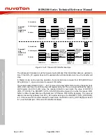
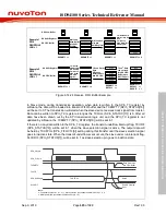
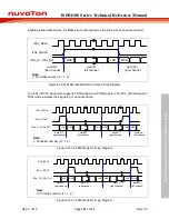
In the example 1 of the following Figure, it indicates the updated condition of TXEMPTY
(SPIn_STATUS[16]) and the relationship among the FIFO buffer, shift register and the skew buffer.
The TXEMPTY (SPIn_STATUS[16]) is set to 0 when the Data0 is written into the FIFO buffer. The
Data0 will be loaded into the shift register by the core logic and the TXEMPTY (SPIn_STATUS[16])
will be to 1. The Data0 in shift register will be shift into skew buffer by bit for transmission until the
transfer is done.
In the Example 2, it indicates the updated condition of TXFULL (SPIn_STATUS[17]) when there
are 8 data in the FIFO buffer and the next data of Data9 does not be written into the FIFO buffer
when the TXFULL = 1.


