ISD94100 Series Technical Reference Manual
Sep 9, 2019
Page
248
of 928
Rev1.09
IS
D
9
410
0
S
ER
IE
S
T
E
C
HN
ICA
L
RE
F
E
RE
NCE
M
AN
U
AL
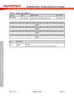
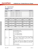
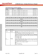
6.5.7
Register Description
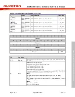
Port A-D I/O Mode Control
(Px_MODE)
Register
Offset
R/W Description
Reset Value
PA_MODE
0x000
R/W PA I/O Mode Control
0xXXXX_XXXX
PB_MODE
0x040
R/W PB I/O Mode Control
0xXX0X_XXXX
PC_MODE
0x080
R/W PC I/O Mode Control
0xXXXX_XXXX
PD_MODE
0x0C0
R/W PD I/O Mode Control
0xXXXX_XXXX
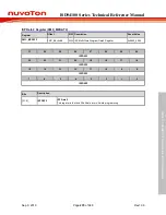
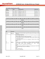
31
30
29
28
27
26
25
24
MODE15
MODE14
MODE13
MODE12
23
22
21
20
19
18
17
16
MODE11
MODE10
MODE9
MODE8
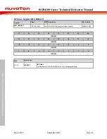
15
14
13
12
11
10
9
8
MODE7
MODE6
MODE5
MODE4
7
6
5
4
3
2
1
0
MODE3
MODE2
MODE1
MODE0
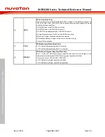
Bits
Description
[2n+1:2n]
n=0,1..15
MODEn
Port A-D I/O Pin[n] Mode Control
Determine each I/O mode of Px.n pins.
00 = Px.n is in Input mode.
01 = Px.n is in Push-pull Output mode.
10 = Px.n is in Open-drain Output mode.
11 = Px.n is in Quasi-bidirectional mode.
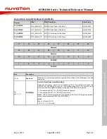
Note 1:
The reset value of this field is defined by CIOINI (CONFIG0[10]) except PA_MODE[17:16].
If CIOINI is set to 0, the reset value is 0xFFFF_FFFF and all pins will be quasi-bidirectional
mode after chip power-on or
reset period.
If CIOINI is set to 1, the reset value is 0x0000_0000 and all pins will be
input mode after chip power-on or reset period.
Note 2:
The reset value of PA_MODE[17:16] field is defined by GPA8_LOW (CONFIG0[11]).
If GPA8_LOW is set to 0, the reset value of PA_MODE[17:16] is 0x1 and PA.8 will be push-
pull output mode after chip power-on or reset period.
If GPA8_LOW is set to 1, the reset value of PA_MODE[17:16] follows CIOINI setting.
Note 3:
Max. n=15 for port A/C/D
n=0..9, 13, 14, 15 for port B

