ISD94100 Series Technical Reference Manual
Sep 9, 2019
Page
694
of 928
Rev1.09
IS
D
9
410
0
S
ER
IE
S
T
E
C
HN
ICA
L
RE
F
E
RE
NCE
M
AN
U
AL
Example 1
SPI0
DWIDTH =0
LSB = 1
TXEMPTY = 1
Data 0
TXEMPTY = 0
Write
1 Data
TXEMPTY = 1
H/W load TX
Buffer into
Shift Register
Data 0
TXEMPTY = 1
Data 0
b0
b1
b2
TXEMPTY = 1
Data 0
TXEMPTY = 0
Write
3 Data
Data 1
TXEMPTY = 0
TXFULL = 1
Data 2
1. H/W load
TX Buffer into
Shift Register
2. Write 6
Data
Data 0
1. H/W load
Shift Register
into Skew
Buffer
2. Write 1 Data
Data 0
b0
b1
b2
Data 1
Data 2
Data 3
Data 4
Data 5
Data 6
Data 7
Data 8
Data 1
Data 2
Data 3
Data 4
Data 5
Data 6
Data 7
Data 8
TXEMPTY = 0
TXFULL = 1
Example 2
SPI0
DWIDTH =0
LSB = 1
TX Buffer
TX Shift Register
TX Skew Buffer
H/W load Shift
Register into
Skew Buffer
TX Buffer
TX Shift Register
TX Skew Buffer
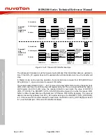
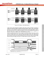
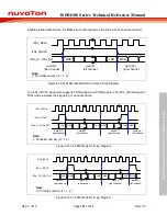
Figure 6.14-23 Transmit FIFO Buffer Example
The subsequent transactions will be triggered automatically if the transmitted data are updated in
time. If the SPIn_TX register does not be updated after all data transfer are done, the transfer will
stop.
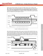
In Master mode, during receiving operation, the serial data are received from SPI0_MISO0 and
SPIx_MISO (x=1, 2) pin and stored to receive FIFO buffer.
The received data (Data0’s b0, b1, …b31) is stored into skew buffer first according the serial clock
(SPIn_CLK) and then it is shift into the shift register bit by bit. The core logic will load the data in
shift register into FIFO buffer when the received data bit count reach the value of DWIDTH
(SPIn_CTL[12:8]). The RXEMPTY (SPIn_STATUS[8]) will be cleared to 0 while the receive FIFO
buffer contains unread data (see the Example 1 of Receive FIFO Buffer Example). The received
data can be read by software from SPIn_RX register as long as the RXEMPTY (SPIn_STATUS[8])
is 0. If the receive FIFO buffer contains 8 unread data, the RXFULL (SPIn_STATUS[9]) will be set
to 1 (see the Example 2 of Receive FIFO Buffer Example).

