ISD94100 Series Technical Reference Manual
Sep 9, 2019
Page
777
of 928
Rev1.09
IS
D
9
410
0
S
ER
IE
S
T
E
C
HN
ICA
L
RE
F
E
RE
NCE
M
AN
U
AL
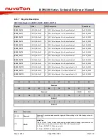
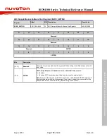
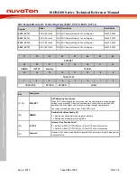
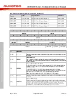
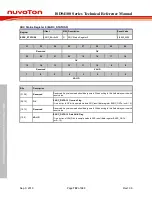
ADC Control Register (EADC_CTL)
Register
Offset
R/W Description
Reset Value
EADC_CTL
0x50
R/W ADC Control Register
0x0000_00C0
31
30
29
28
27
26
25
24
Reserved
23
22
21
20
19
18
17
16
Reserved
15
14
13
12
11
10
9
8
Reserved
PDMAEN
Reserved
DMOF
Reserved
7
6
5
4
3
2
1
0
RESSEL
ADCIEN3
ADCIEN2
ADCIEN1
ADCIEN0
ADCRST
ADCEN
Bits
Description
[31:12]
Reserved
Reserved. Any values read should be ignored. When writing to this field always write with reset
value.
[11]
PDMAEN
PDMA Transfer Enable Bit
When ADC conversion is completed, the converted data is loaded into EADC_DATn (n: 0 ~ 12)
register, user can enable this bit to generate a PDMA data transfer request.
0 = PDMA data transfer Disabled.
1 = PDMA data transfer Enabled.
Note:
When set this bit field to 1, user must set ADCIENn (EADC_CTL[5:2], n=0~3) = 0 to
disable interrupt.
[10]
Reserved
Reserved. Any values read should be ignored. When writing to this field always write with reset
value.
[9]
DMOF
ADC Differential Input Mode Output Format
0 = ADC conversion result will be filled in RESULT (EADC_DATn[15:0] , n= 0 ~12) with
unsigned format.
1 = ADC conversion result will be filled in RESULT (EADC_DATn[15:0] , n= 0 ~12) with
2’complement format.
[8]
Reserved
Reserved. Any values read should be ignored. When writing to this field always write with reset
value.
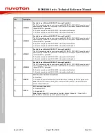
[7:6]
RESSEL
Resolution Selection
00 = 6-bit. ADC result will put at RESULT (EADC_ DATn [5:0]).
01 = 8-bit. ADC result will put at RESULT (EADC_ DATn [7:0]).
10 = 10-bit. ADC result will put at RESULT (EADC_ DATn [9:0]).
11 = 12-bit. ADC result will put at RESULT (EADC_ DATn [11:0]).

