ISD94100 Series Technical Reference Manual
Sep 9, 2019
Page
682
of 928
Rev1.09
IS
D
9
410
0
S
ER
IE
S
T
E
C
HN
ICA
L
RE
F
E
RE
NCE
M
AN
U
AL
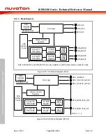
SPIx_CLK
SPIx_MISO
SPIx_MOSI
SPIx_SS
SPI_CLK
SPI_DO
SPI_DI
SPI_SS
Note: x = 1, 2
I94100 Series
SPI Master
Slave
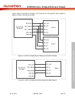
Figure 6.14-7 SPI1 ~ SPI2 Full-Duplex Master Mode Application Block Diagram
SPIx_CLK
SPIx_MISO
SPIx_MOSI
SPIx_SS
SPI_CLK
SPI_DI
SPI_DO
SPI_SS
Note: x = 1, 2
I94100 Series
SPI Slave
Master
Figure 6.14-8 SPI1 ~ SPI2 Full-Duplex Slave Mode Application Block Diagram
Slave Selection
In Master mode, the SPI controller can drive off-chip slave device through the slave select output
pin SPI0_SSy (y=0, 1) and SPIn_SS (n=1, 2). In Slave mode, the off-chip master device drives the
slave selection signal from the SPI0_SS0 and SPIn_SS (n=1, 2) input port to this SPI controller.
The duration between the slave select active edge and the first SPI clock input shall over 3 SPI
peripheral clock cycles of slave.
In Master/Slave mode, the active state of slave selection signal can be programmed to low or high
active in SSACTPOL (SPIn_SSCTL[2]). The selection of slave select conditions depends on what
type of device is connected. In Slave mode, to recognize the inactive state of the slave selection
signal, the inactive period of the slave selection signal must be larger than or equal to 3 peripheral
clock cycles between two successive transactions.
Timing Condition
The CLKPOL (SPIn_CTL[3]) defines the SPI clock idle state. If CLKPOL = 1, the output SPI clock
is idle at high state; if CLKPOL = 0, it is idle at low state.
TXNEG (SPIn_CTL[2]) defines the data transmitted out either on negative edge or on positive edge
of SPI clock. RXNEG (SPIn_CTL[1]) defines the data received either on negative edge or on

