ISD94100 Series Technical Reference Manual
Sep 9, 2019
Page
391
of 928
Rev1.09
IS
D
9
410
0
S
ER
IE
S
T
E
C
HN
ICA
L
RE
F
E
RE
NCE
M
AN
U
AL
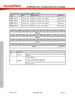
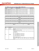
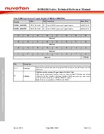
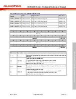
Timer PWM Output Mask Data Control Register (TIMERx PWMMSK)
Register
Offset
R/W Description
Reset Value
TIMER0_PWMMSK
T0x64
R/W Timer0 PWM Output Mask Data Control Register
0x0000_0000
TIMER1_PWMMSK
T0x164
R/W Timer1 PWM Output Mask Data Control Register
0x0000_0000
TIMER2_PWMMSK
T0x64
R/W Timer2 PWM Output Mask Data Control Register
0x0000_0000
TIMER3_PWMMSK
T0x164
R/W Timer3 PWM Output Mask Data Control Register
0x0000_0000
31
30
29
28
27
26
25
24
Reserved
23
22
21
20
19
18
17
16
Reserved
15
14
13
12
11
10
9
8
Reserved
7
6
5
4
3
2
1
0
Reserved
MSKDAT1
MSKDAT0
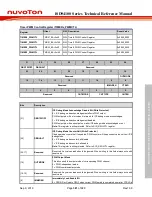
Bits
Description
[31:2]
Reserved
Reserved. Any values read should be ignored. When writing to this field always write with
reset value.
[1]
MSKDAT1
PWMx_CH1 Output Mask Data Control Bit
This bit is used to control the output state of PWMx_CH1 pin when PWMx_CH1 output mask
function is enabled (MSKEN1 = 1).
0 = Output logic Low to PWMx_CH1.
1 = Output logic High to PWMx_CH1.
[0]
MSKDAT0
PWMx_CH0 Output Mask Data Control Bit
This bit is used to control the output state of PWMx_CH0 pin when PWMx_CH0 output mask
function is enabled (MSKEN0 = 1).
0 = Output logic Low to PWMx_CH0.
1 = Output logic High to PWMx_CH0.


