ISD94100 Series Technical Reference Manual
Sep 9, 2019
Page
686
of 928
Rev1.09
IS
D
9
410
0
S
ER
IE
S
T
E
C
HN
ICA
L
RE
F
E
RE
NCE
M
AN
U
AL
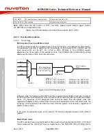
Byte3
Byte0
Byte1
Byte2
SPI_TX/SPI_RX
TX/RX FIFO Buffer
LSB = 0 (MSB first)
& REORDER = 1
DWIDTH = 24
DWIDTH = 16
DWIDTH = 0
MSB first
MSB first
x = unknown byte
x
Byte1
Byte0
x
Byte1
Byte0
x
Byte2
MSB first
Byte3
Byte0 Byte1 Byte2
MSB first
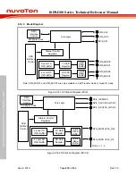
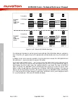
Figure 6.14-12 Byte Reorder Function
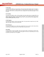
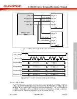
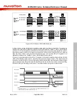
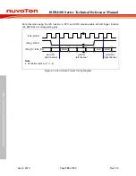
In Master mode, if REORDER (SPIn_CTL[19]) is set to 1, a suspend interval of 0.5 ~ 15.5 SPI clock
periods will be inserted by hardware between two successive bytes in a transaction word. The
suspend interval is configured in SUSPITV (SPIn_CTL[7:4]).
SPIx_CLK pin
SPIx_MISOz pin
SPIx_MOSIz pin
TX[6]
TX[0]
TX[15]
TX[14]
TX[8]
RX[6]
RX[0]
RX[14]
RX[8]
MSB
RX[7]
Suspend
Interval
1st Transaction Byte
2nd Transaction Byte
RX[15]
MSB
TX[7]
Note:
Timing Condition is CLKPOL = 0, LSB = 0, TXNEG = 1, DWIDTH = 0, REORDER = 1 and SLAVE = 0
x: Controller number (x = 0, 1, 2), z: MOSI and MISO pin channel number in SPI0 (z = 0, 1)
Figure 6.14-13 Timing Waveform for Byte Suspend
6.14.5.4 Half-Duplex Communication
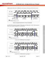
The SPI controller can communicate in half-duplex mode by setting HALFDPX (SPIn_CTL[14]) bit.
In half-duplex mode, there is only one data line for receiving or transmitting data direction which is
defined by DATDIR (SPIn_CTL[20]). In half-duplex configuration, the SPI0_MISO0 and SPIx_MISO
(x=1, 2) pin is free for other applications and it can be configured as GPIO. Enabling or disabling
the control bit HALFDPX (SPIn_CTL[14]) will produce TXRST (SPIn_FIFOCTL[1]) and RXRST
(SPIn_FIFOCTL[0]) at the same time automatically.

