ISD94100 Series Technical Reference Manual
Sep 9, 2019
Page
724
of 928
Rev1.09
IS
D
9
410
0
S
ER
IE
S
T
E
C
HN
ICA
L
RE
F
E
RE
NCE
M
AN
U
AL
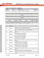
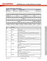
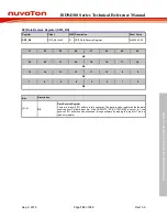
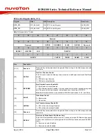
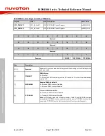
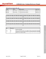
SPI Control Register (SPIn_CTL)
Register
Offset
R/W Description
Reset Value
SPI1_CTL
0x00
R/W SPI1 Control Register
0x0000_0034
SPI2_CTL
0x00
R/W SPI2 Control Register
0x0000_0034
Note:
Not supported in I
2
S mode.
31
30
29
28
27
26
25
24
Reserved
23
22
21
20
19
18
17
16
Reserved
DATDIR
REORDER
SLAVE
UNITIEN
Reserved
15
14
13
12
11
10
9
8
RXONLY
HALFDPX
LSB
DWIDTH
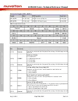
7
6
5
4
3
2
1
0
SUSPITV
CLKPOL
TXNEG
RXNEG
SPIEN
Bits
Description
[31:21]
Reserved
Reserved. Any values read should be ignored. When writing to this field always write with
reset value.
[20]
DATDIR
Data Port Direction Control
This bit is used to select the data input/output direction in half-duplex transfer and Dual/Quad
transfer
0 = SPI data is input direction.
1 = SPI data is output direction.
[19]
REORDER
Byte Reorder Function Enable Bit
0 = Byte Reorder function Disabled.
1 = Byte Reorder function Enabled. A byte suspend interval will be inserted among each
byte. The period of the byte suspend interval depends on the setting of SUSPITV.
Note:
Byte Reorder function is only available if DWIDTH is defined as 16, 24, and 32 bits.
[18]
SLAVE
Slave Mode Control
0 = Master mode.
1 = Slave mode.
[17]
UNITIEN
Unit Transfer Interrupt Enable Bit
0 = SPI unit transfer interrupt Disabled.
1 = SPI unit transfer interrupt Enabled.
[16]
Reserved
Reserved. Any values read should be ignored. When writing to this field always write with
reset value.
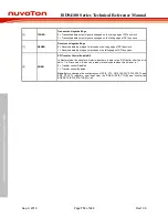
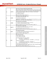
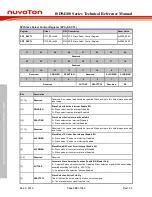
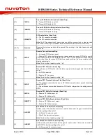
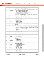
[15]
RXONLY
Receive-only Mode Enable Bit (Master Only)
This bit field is only available in Master mode. In receive-only mode, SPI Master will generate
SPI bus clock continuously for receiving data bit from SPI slave device and assert the BUSY
status.
0 = Receive-only mode Disabled.
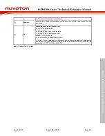
1 = Receive-only mode Enabled.


