ISD94100 Series Technical Reference Manual
Sep 9, 2019
Page
785
of 928
Rev1.09
IS
D
9
410
0
S
ER
IE
S
T
E
C
HN
ICA
L
RE
F
E
RE
NCE
M
AN
U
AL
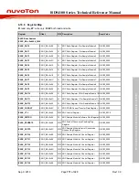
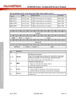
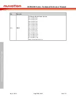
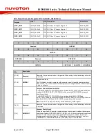
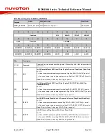
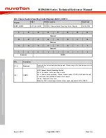
ADC Sample Module 4~12 Control Registers (EADC_SCTL4~EADC_SCTL12)
Register
Offset
R/W Description
Reset Value
EADC_SCTL4
0x90
R/W ADC Sample Module 4 Control Register
0x0000_0000
EADC_SCTL5
0x94
R/W ADC Sample Module 5 Control Register
0x0000_0000
EADC_SCTL6
0x98
R/W ADC Sample Module 6 Control Register
0x0000_0000
EADC_SCTL7
0x9C
R/W ADC Sample Module 7 Control Register
0x0000_0000
EADC_SCTL8
0xA0
R/W ADC Sample Module 8 Control Register
0x0000_0000
EADC_SCTL9
0xA4
R/W ADC Sample Module 9 Control Register
0x0000_0000
EADC_SCTL10
0xA8
R/W ADC Sample Module 10 Control Register
0x0000_0000
EADC_SCTL11
0xAC
R/W ADC Sample Module 11 Control Register
0x0000_0000
EADC_SCTL12
0xB0
R/W ADC Sample Module 12 Control Register
0x0000_0000
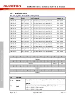
31
30
29
28
27
26
25
24
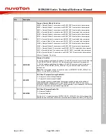
EXTSMPT
23
22
21
20
19
18
17
16
Reserved
INTPOS
Reserved
TRGSEL
15
14
13
12
11
10
9
8
TRGDLYCNT
7
6
5
4
3
2
1
0
TRGDLYDIV
EXTFEN
EXTREN
CHSEL
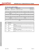
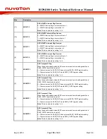
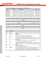
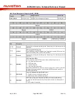
Bits
Description
[31:24]
EXTSMPT
ADC Sampling Time Extend
When ADC converting at high conversion rate, the sampling time of analog input
voltage may not enough if input channel loading is heavy, SW can extend ADC
sampling time after trigger source is coming to get enough sampling time.
The range of start delay time is from 0~255 ADC clock.
[23]
Reserved
Reserved. Any values read should be ignored. When writing to this field always write
with reset value.
[22]
INTPOS
Interrupt Flag Position Select
0 = Set ADIFn (EADC_STATUS2[n], n=0~3) at ADC end of conversion.
1 = Set ADIFn (EADC_STATUS2[n], n=0~3) at ADC start of conversion.
[21]
Reserved
Reserved. Any values read should be ignored. When writing to this field always write
with reset value.

