ISD94100 Series Technical Reference Manual
Sep 9, 2019
Page
145
of 928
Rev1.09
IS
D
9
410
0
S
ER
IE
S
T
E
C
HN
ICA
L
RE
F
E
RE
NCE
M
AN
U
AL
6.3.4
Peripheral Clock
Each peripheral module can have its own clock source selection and configuration, please refer to
CLK_CLKSEL1 and CLK_CLKSEL2 register description for more detailed information.
6.3.5
Power-down Mode Clock
Different power down modes have different impact on the system clocks. Under a certain power
down mode, some clock sources (including system clocks and peripheral clocks) are disabled
while some other clock sources are still available. However regardless the power down mode the
following clocks are always available:
Clock Generator
10 kHz internal low speed RC oscillator (LIRC) clock
32.768 kHz external low speed crystal oscillator (LXT) clock
Peripheral Clock which uses LXT or LIRC as clock source
6.3.6
Clock Output
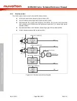
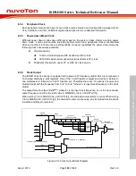
The ISD94100 series device is equipped with a power-of-2 frequency divider which is composed of
16 chained divide-by-2 shift registers. One of the 16 shift register outputs selected by a sixteen to
one multiplexer is reflected to CLKO function pin. Therefore there are 16 options of power-of-2
divided clocks with the frequency from F
in
/2
1
to F
in
/2
16
where F
in
is input clock frequency to the clock
divider.
The output formula is
F
out
= F
in
/2
(N+1)
,
where F
in
is the input clock frequency, F
out
is the clock divider
output frequency and N is the 4-bit value in FREQSEL (CLK_CLKOCTL[3:0]).
When writing 1 to CLKOEN (CLK_CLKOCTL[4]), the chained counter starts to count. When writing
0 to CLKOEN (CLK_CLKOCTL[4]), the chained counter continuously runs till divided clock reaches
low state and stays in low state.
0000
0001
1110
1111
:
:
16 to 1
MUX
1/2
1/2
2
1/2
3
1/2
15
1/2
16
…...
FREQSEL
(CLK_CLKOCTL[3:0])
CLKO
16 chained
divide-by-2 counter
CLKOEN
(CLK_CLKOCTL[4])
Enable
divide-by-2 counter
0
1
DIV1EN
(CLK_CLKOCTL[5])
0
1
CLK1HZEN
(CLK_CLKOCTL[6])
1 Hz clock from RTC
1
0
LXT
LIRC
RTCSEL(CLK_CLKSEL3[8])
/32768
11
HCLK
LXT
HXT
HIRC
CLKOSEL (CLK_CLKSEL1[29:28])
10
01
00
/10000
Figure 6.3-6 Clock Output Block Diagram
Содержание ISD94100 Series
Страница 528: ...ISD94100 Series Technical Reference Manual Sep 9 2019 Page 528 of 928 Rev1 09 ISD94100 SERIES TECHNICAL REFERENCE MANUAL...
Страница 626: ...ISD94100 Series Technical Reference Manual Sep 9 2019 Page 626 of 928 Rev1 09 ISD94100 SERIES TECHNICAL REFERENCE MANUAL...
Страница 702: ...ISD94100 Series Technical Reference Manual Sep 9 2019 Page 702 of 928 Rev1 09 ISD94100 SERIES TECHNICAL REFERENCE MANUAL...
Страница 875: ...ISD94100 Series Technical Reference Manual Sep 9 2019 Page 875 of 928 Rev1 09 ISD94100 SERIES TECHNICAL REFERENCE MANUAL...


