background image


ISD94100 Series Technical Reference Manual 


Sep 9, 2019 

Page 

683

 of 928 

Rev1.09 

IS

D

9

410

0

 S

ER
IE


T

E

C

HN

ICA
L

 RE

F

E

RE

NCE

 M

AN
U

AL


positive edge of SPI clock. 

Note:

 The settings of TXNEG and RXNEG are mutual exclusive. In other words, do not transmit 

and receive data at the same clock edge. 


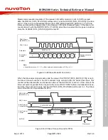
Transmit/Receive Bit Length 

The bit length of a transaction word is defined in DWIDTH (SPIn_CTL[12:8]) and can be configured 
up to 32-bit length in a transaction word for transmitting and receiving. 

When SPI controller finishes a transaction, i.e. receives or transmits a specific count of bits defined 
in DWIDTH (SPIn_CTL[12:8]), the unit transfer interrupt flag will be set to 1. 


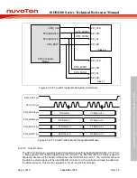
SPIx_CLK pin

SPIx_MOSIz pin

SPIx_MISOz pin

TX[30]

TX[16]

TX[15] TX[14]

LSB

TX[0]

RX[30]

RX[16]

RX[14]

LSB

RX[0]

MSB

RX[31]

RX[15]

MSB

TX[31]

SPIx_SSy pin

Note:

x: Controller number (x = 0, 1, 2), y: Slave selection pin channel number in SPI0 (y = 0, 1), 
z: MOSI and MISO pin channel number in SPI0 (z = 0) 


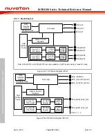
Figure 6.14-9 32-Bit in One Transaction 


LSB/MSB First 

LSB (SPIn_CTL[13]) defines the bit transfer sequence in a transaction. If the LSB (SPIn_CTL[13]) 
is set to 1, the transfer sequence is LSB first. The bit 0 will be transferred firstly. If the LSB 
(SPIn_CTL[13]) is cleared to 0, the transfer sequence is MSB first. 


Suspend Interval 

SUSPITV (SPIn_CTL[7:4]) provides a configurable suspend interval, 0.5 ~ 15.5 SPI clock periods, 
between two successive transaction words in Master mode. The definition of the suspend interval 
is the interval between the last clock edge of the preceding transaction word and the first clock edge 
of the following transaction word. The default value of SUSPITV is 0x3 (3.5 SPI clock cycles). 


6.14.5.2  Automatic Slave Selection 

In Master mode, if AUTOSS (SPIn_SSCTL[3]) is set, the slave selection signal will be generated 
automatically and output to the slave selection pin according to whether SS (SPIn_SSCTL[0]) and 
SS1 (SPI0_SSCTL[1]) is enabled or not. The slave selection signal will be set to active state by the 
SPI controller when the SPI data transfer is started by writing to FIFO. It will be set to inactive state 
when SPI bus is idle. If SPI bus is not idle, i.e. TX FIFO, TX shift register or TX skew buffer is not 
empty, the slave selection signal will be set to inactive state between transactions if the value of 

Содержание ISD94100 Series

Страница 1: ...intellectual property of Nuvoton Technology Corporation and shall not be reproduced without permission from Nuvoton Nuvoton is providing this document only for reference purposes of microcontroller b...

Страница 2: ...x10 mm Pin Diagram 33 4 4 Pin Description 34 4 5 GPIO Alternate Function Summary 43 5 BLOCK DIAGRAM 45 5 1 ISD94100 Series Block Diagram 45 6 FUNCTIONAL DESCRIPTION 46 6 1 ARM Cortex M4 Core 46 6 2 Sy...

Страница 3: ...6 4 Flash Memory Controller FMC 191 6 4 1 Overview 191 6 4 2 Features 191 6 4 3 Block Diagram 192 6 4 4 Functional Description 194 6 4 5 Register Map 215 6 4 6 Register Description 217 6 5 General Pu...

Страница 4: ...lock Diagram 404 6 8 4 Basic Configuration 407 6 8 5 Functional Description 408 6 8 6 Register Map 439 6 8 7 Register Description 443 6 9 Watchdog Timer WDT 525 6 9 1 Overview 525 6 9 2 Features 525 6...

Страница 5: ...Map 588 6 12 7 Register Description 589 6 13 I2 C Serial Interface Controller I2 C 617 6 13 1 Overview 617 6 13 2 Features 617 6 13 3 Block Diagram 617 6 13 4 Basic Configuration 618 6 13 5 Functional...

Страница 6: ...egister Description 774 6 17 I2 S Controller I2 S 801 6 17 1 Overview 801 6 17 2 Features 801 6 17 3 Block Diagram 802 6 17 4 Basic Configuration 802 6 17 5 Functional Description 803 6 17 6 Register...

Страница 7: ...6 20 6 Register Map 885 6 20 7 Register Description 886 6 21 Audio DPWM Modulator DPWM 897 6 21 1 Overview 897 6 21 2 Features 897 6 21 3 Block Diagram 897 6 21 4 Basic Configuration 897 6 21 5 Functi...

Страница 8: ...m 142 Figure 6 3 3 System Clock Block Diagram 143 Figure 6 3 4 HXT Stop Protect Procedure 144 Figure 6 3 5 SysTick Clock Control Block Diagram 144 Figure 6 3 6 Clock Output Block Diagram 145 Figure 6...

Страница 9: ...7 1 Timer Controller Block Diagram 340 Figure 6 7 2 Clock Source of Timer Controller 341 Figure 6 7 3 PWM Generator Overview Block Diagram 342 Figure 6 7 4 PWM System Clock Source Control 342 Figure...

Страница 10: ...8 6 PWM0_CH0 Prescaler Waveform in Up Counter Type 408 Figure 6 8 7 PWM0 Counter Waveform when set clear counter 409 Figure 6 8 8 PWM Up Counter Type 409 Figure 6 8 9 PWM Down Counter Type 410 Figure...

Страница 11: ...Operation Waveform 436 Figure 6 8 42 Capture PDMA Operation Waveform of Channel 0 438 Figure 6 9 1 Watchdog Timer Block Diagram 525 Figure 6 9 2 Watchdog Timer Clock Control 526 Figure 6 9 3 Watchdog...

Страница 12: ...Master Reads Data from Slave by 10 bit 624 Figure 6 13 12 Control I2C Bus according to the current I2C Status 625 Figure 6 13 13 Master Transmitter Mode Control Flow 627 Figure 6 13 14 Master Receive...

Страница 13: ...Two Bit Transfer Mode Timing Master Mode 689 Figure 6 14 18 Bit Sequence of Dual Output Mode 690 Figure 6 14 19 Bit Sequence of Dual Input Mode 690 Figure 6 14 20 Bit Sequence of Quad Output Mode 691...

Страница 14: ...6 16 14 ADC Controller Interrupts 768 Figure 6 16 15 ADC start up sequence with calibration 769 Figure 6 16 16 Model of the sampling network 770 Figure 6 17 1 I2S Controller Block Diagram 802 Figure 6...

Страница 15: ...eration Flow 836 Figure 6 18 3 Endpoint SRAM Structure 837 Figure 6 18 4 Setup Transaction Followed by Data IN Transaction 837 Figure 6 18 5 Data Out Transfer 838 Figure 6 19 1 DMIC Block Diagram 866...

Страница 16: ...Table 6 3 9 1 The symbol definition of PLL Output Frequency formula 167 Table 6 4 4 1 Flash Memory Address Map 195 Table 6 4 4 2 Boot Configuration 196 Table 6 4 4 3 ISP Command List 201 Table 6 4 4 4...

Страница 17: ...tion Example Table 1 573 Table 6 12 5 5 Baud Rate Compensation Example Table 2 573 Table 6 12 5 6 UART controller Interrupt Source and Flag List 580 Table 6 12 5 7 UART Line Control of Word and Stop L...

Страница 18: ...product applications which need communication interfaces and high computing power The ISD94100 is also equipped with a variety of peripheral devices such as Multi Function Timers Watchdog Timers RTC...

Страница 19: ...system program ISP In application program IAP update Supports 4 KB page erase for all embedded flash Supports 4 KB two way cache to reduce power consumption and improve performance Enhanced performanc...

Страница 20: ...ter Gather Transfer modes Each channel supports circular buffer management using Scatter Gather Transfer mode Supports two types of priorities modes Fixed priority and Round robin modes Supports byte...

Страница 21: ...h PWM channel Supports trigger EADC to start conversion Supports up to 6 independent input capture channels with 16 bit resolution counter Watchdog Timer 18 bit free running up counter for WDT time ou...

Страница 22: ...Baud Rate measurement and baud rate compensation function Supports break error frame error parity error and receive transmit FIFO overflow detection function Supports nCTS incoming data RX FIFO reache...

Страница 23: ...Dual and Quad I O Transfer mode Supports one two data channel half duplex transfer Support receive only mode Configurable bit length of a transfer word from 8 to 32 bit Provides separate 8 level dept...

Страница 24: ...tware enable External pin Timer 0 3 overflow pulse trigger and PWM trigger 12 bit 10 bit 8 bit 6 bit configurable resolution Maximum EADC clock frequency is 60 MHz Configurable EADC internal sampling...

Страница 25: ...ng point for input data and BIQ coefficient Provides one 32 level FIFO data buffers for transmitting Cyclic Redundancy Calculation Unit Supports four common polynomials CRC CCITT CRC 8 CRC 16 and CRC...

Страница 26: ...udio DPWM Modulator EBI External Bus Interface EPWM Enhanced Pulse Width Modulation FIFO First In First Out FMC Flash Memory Controller FPU Floating point Unit GPIO General Purpose Input Output HCLK T...

Страница 27: ...ure Encoder Interface SD Secure Digital SPI Serial Peripheral Interface SPS Samples per Second TDES Triple Data Encryption Standard TMR Timer Controller UART Universal Asynchronous Receiver Transmitte...

Страница 28: ...I 13 BYI Max CPU frequency MHz 100 200 Flash KB 512 256 512 256 SRAM KB 192 128 192 128 ISP Loader ROM KB 4 I O 58 57 41 32 bit Timer 4 RTC Connectivity UART 1 SPI 1 SPI I2 S 2 I2 S 1 I2 C 2 PWM 6 5 U...

Страница 29: ...6x6 mm D LQFP64 7x7 mm R LQFP64 10x10 mm Family ID 1 Family Series ID Temperature I 40 85 Product Series 4 Cortex M4F Flash ROM Feature A Standard B Basic no Audio C Standard Voice Recognition D Stan...

Страница 30: ...KB 512 KB Standard feature LQFP64 7x7 mm ISD94124CDI 192 KB 512 KB Standard feature VR LQFP64 7x7 mm ISD94124DDI 192 KB 512 KB Standard feature BF NR LQFP64 7x7 mm ISD94124PDI 192 KB 512 KB Standard...

Страница 31: ...PB 4 nRESET PB 5 PB 6 LDO_CAP VSS AVSS VDD 24 23 22 21 20 19 18 17 16 15 14 13 PD 1 PD 0 PB 13 PB 14 PB 15 USB_VDD33 PC 4 PC 3 PC 2 PC 1 PC 0 AVDD 36 35 34 33 32 31 30 29 28 27 26 25 PA 3 PA 2 PA 1 PA...

Страница 32: ...14 PB 9 PC 11 PC 9 PC 8 PC 7 PD 3 PD 8 PD 4 PD 2 PA 2 PA 4 PD 15 PA 8 PD 1 PD 0 PA 3 PA 7 PA 6 PA 9 PD 14 PB 6 PA 5 1 2 3 4 5 6 7 8 9 10 11 12 48 47 46 45 44 43 42 41 40 39 38 37 17 18 19 20 21 22 23...

Страница 33: ...4 PB 9 PC 11 PC 9 PC 8 PC 7 PD 6 PD 11 PD 7 PD 5 PA 2 PA 4 PD 15 PA 8 PD 4 PD 3 PA 3 PA 7 PA 6 PA 9 PD 14 PB 6 PA 5 1 2 3 4 5 6 7 8 9 10 11 12 48 47 46 45 44 43 42 41 40 39 38 37 17 18 19 20 21 22 23...

Страница 34: ...output PWM0_CH2 I O MFP3 PWM0 channel2 output capture input 4 4 4 PB 3 I O MFP0 General purpose digital I O pin PWM0_CH1 I O MFP1 PWM0 channel1 output capture input TM2_EXT I O MFP2 Timer2 external ca...

Страница 35: ...e digital I O pin UART0_RXD I MFP1 UART0 Data receiver input pin PWM0_CH5 I O MFP2 PWM0 channel5 output capture input 9 12 12 LDO_CAP P MFP0 LDO output pin Note This pin needs to be connected with a 1...

Страница 36: ...I MFP1 External interrupt2 input pin SPI2_MISO I O MFP2 SPI2 MISO Master In Slave Out pin 24 24 PC 7 I O MFP0 General purpose digital I O pin SPI0_SS0 I O MFP1 1st SPI0 Slave Select pin SPI2_CLK I O...

Страница 37: ...FP0 Power supply for USB DC 3 3V 20 33 PB 15 I O MFP0 General purpose digital I O pin USB_VBUS P MFP1 Power supply from USB or HUB I2S0_MCLK O MFP2 I2S0 master clock output pin 21 34 PB 14 I O MFP0 Ge...

Страница 38: ...put bit1 SPI1_CLK I O MFP2 SPI1 serial clock pin I2S0_DI I MFP3 I2S0 data input pin DMIC_DAT1 I MFP4 Digital microphone channel 1 data input pin TM1 I O MFP5 Timer1 event counter input toggle output 2...

Страница 39: ...gger input 44 PD 11 I O MFP0 General purpose digital I O pin UART0_TXD O MFP1 UART0 Data transmitter output pin INT2 I MFP2 External interrupt2 input pin 45 PD 12 I O MFP0 General purpose digital I O...

Страница 40: ...icrophone channel 1 data input pin 36 52 52 PA 3 I O MFP0 General purpose digital I O pin SPI0_MOSI0 I O MFP1 1st SPI0 MOSI Master Out Slave In pin EADC0_CH3 A MFP2 EADC0 channel3 analog input DMIC_CL...

Страница 41: ...PA 11 I O MFP0 General purpose digital I O pin I2C0_SMBSUS O MFP1 I2C0 SMBus SMBSUS pin PMBus CONTROL pin TM0 I O MFP2 Timer0 event counter input toggle output DPWM_RP O MFP3 Audio DPWM right channel...

Страница 42: ...hnical Reference Manual Sep 9 2019 Page 42 of 928 Rev1 09 ISD94100 SERIES TECHNICAL REFERENCE MANUAL Note 1 Part number ISD941XXBYI and ISD941XXBRI do not provide DPWM and DMIC functionality Table 4 4...

Страница 43: ...PI0_SS0 EADC0_CH6 PA 7 UART0_TXD EADC0_CH7 SPI2_MISO PA 8 UART0_RXD EADC0_CH8 SPI2_MOSI PA 9 I2C0_SCL EADC0_CH9 SPI2_SS PA 10 I2C0_SDA EADC0_ST DPWM_RN SPI2_CLK PA 11 I2C0_SMBSUS TM0 DPWM_RP PA 12 I2C...

Страница 44: ..._SCL I2S0_BCLK DPWM_LN PD 1 INT4 I2C1_SDA I2C0_SDA I2S0_LRCK DPWM_LP PD 2 TRACE_CLK SPI1_MOSI I2S0_MCLK I2C1_SCL TM0 PD 3 TRACE_DATA0 SPI1_MISO I2S0_LRCK DMIC_CLK1 TM2 PD 4 TRACE_DATA1 SPI1_CLK I2S0_D...

Страница 45: ...OM POR LVR BOD CPU core LDO 1 2V Memory Power control Timer PWM Timer x4 WDT x1 WWDT x1 PWM x6 RTC Analog Interface 12 bit ADC 13 ch HS Osc 48 0 49 152MHz LS Osc 10KHz PLL 100 500MHz HS Ext Crystal 4...

Страница 46: ...result of an exception An exception return can only be issued in Handler mode Thread mode is entered on Reset and can be entered as a result of an exception return The Cortex M4F is a processor with t...

Страница 47: ...double word registers Decoupled three stage pipeline Nested Vectored Interrupt Controller NVIC closely integrated with the processor core to achieve low latency interrupt processing Features include...

Страница 48: ...for implementing watchpoints data tracing and system profiling Optional Instrumentation Trace Macrocell ITM for support of printf style debugging Optional Trace Port Interface Unit TPIU for bridging...

Страница 49: ...re Reset Sources Power on Reset Low level on the nRESET pin Watchdog Time out Reset and Window Watchdog Reset WDT WWDT Reset Low Voltage Reset LVR Brown out Detector Reset BOD Reset CPU Lockup Reset S...

Страница 50: ...d from CONFIG0 Reload from CONFIG0 Reload from CONFIG0 Reload from CONFIG0 Reload from CONFIG0 BODVL SYS_BODCTL 18 16 BODRSTEN SYS_BODCTL 3 HXTEN CLK_PWRCTL 0 Reload from CONFIG0 Reload from CONFIG0 R...

Страница 51: ...Reload from CONFIG0 Reload from CONFIG0 Reload from CONFIG0 VECMAP FMC_ISPSTS 23 9 Reload based on CONFIG0 Reload based on CONFIG0 Reload based on CONFIG0 Reload based on CONFIG0 Reload based on CONF...

Страница 52: ...VDD voltage rises back and has been above VLVR By default Low Voltage Reset is enabled without De glitch function 6 2 2 4 Brown out Detector Reset BOD Reset Writing 1 to Brown out Detector Enable Bit...

Страница 53: ...ing 1 to CHIPRST bit SYS_IPRST0 1 triggers a CHIP Reset MCU Reset is similar to CHIP Reset as the only difference is that MCU Reset does not reload BS FMC_ISPCTL 1 from CONFIG0 so where device will bo...

Страница 54: ...33 PLL Flash Power On Control PB 5 PB 6 GPIOs except PB 13 PB 15 1 2V LDO_CAP 1uF I94100 Series Power Distribution PC 0 PC 1 V SS POR12 IO Cell 10 KHz LIRC Oscillator 48 0 49 152 MHz HIRC Oscillator 3...

Страница 55: ...o Normal mode and program execution continues In system wake up phase besides waiting for LDO recovery and clock sources are enabled and stable system also needs to wait for LDO voltage rising to the...

Страница 56: ...1 20 Most clocks are disabled except LIRC LXT and only RTC WDT Timer UART peripheral clocks still enable if their clock sources are selected as LIRC LXT Low leakage Power down mode LLPD CPU enters Dee...

Страница 57: ...ined Entry Condition Chip is in normal mode after system reset released CPU executes WFI instruction CPU sets sleep mode enable and power down enable and executes WFI instruction Wake up Sources N A A...

Страница 58: ...N ON Halt Halt FLASH ON ON Halt Halt Halt TIMER ON ON ON OFF3 Halt Halt WDT ON ON ON OFF4 Halt Halt RTC ON ON ON OFF5 ON OFF5 Halt UART ON ON ON OFF6 Halt Halt Others ON ON Halt Halt Halt Table 6 2 5...

Страница 59: ...OR POR Reset Y Y N After software writes 1 to clear PORF SYS_RSTSTS 0 INT External Interrupt Y N N After software write 1 to clear the Px_INTSRC n bit GPIO GPIO Interrupt Y N N After software write 1...

Страница 60: ...1 to clear RS485WKF UARTx_WKSTS 3 Received FIFO Threshold Time out Wake up Y N N After software writes 1 to clear TOUTWKF UARTx_WKSTS 4 I2 C Address match wake up Y N N After software writes 1 to cle...

Страница 61: ...ector and low voltage reset controller will consume less power but the detection speed will become slow The response time is about 13ms When using brown out detector and low voltage reset controller t...

Страница 62: ...Peripheral DMA Control Registers 0x4000_C000 0x4000_CFFF FMC_BA Flash Memory Control Registers 0x4003_1000 0x4003_1FFF CRC_BA CRC Generator Registers APB Controllers Space 0x4000_0000 0x400F_FFFF 0x4...

Страница 63: ...Address Space Assignments for On Chip Controllers 6 2 8 SRAM Memory Organization The ISD94100 series supports up to 192 KB of embedded SRAM and the SRAM organization is separated to two banks SRAM ban...

Страница 64: ...NTCTL 0 is set to 1 When SRAM parity error occurs chip will stop detecting SRAM parity errors until user writes 1 to clear the PERRIF SYS_SRAM_STATUS 0 bit 6 2 9 HIRC Auto Trim This chip supports auto...

Страница 65: ...ISD94100 Series Technical Reference Manual Sep 9 2019 Page 65 of 928 Rev1 09 ISD94100 SERIES TECHNICAL REFERENCE MANUAL...

Страница 66: ...High Byte Multiple Function Control Register 0x0000_0000 SYS_GPC_MFPL SYS_BA 0x40 R W GPIOC Low Byte Multiple Function Control Register 0x0000_0000 SYS_GPC_MFPH SYS_BA 0x44 R W GPIOC High Byte Multip...

Страница 67: ...eset Value SYS_PDID SYS_BA 0x00 R Part Device Identification Number Register 0x1DXX_05XX 1 1 Every part number has a unique default reset value 31 30 29 28 27 26 25 24 PDID 23 22 21 20 19 18 17 16 PDI...

Страница 68: ...t Note Write 1 to clear this bit to 0 Note when ICE is connected CPU lockup event sets this flag to 1 but will not reset chip 7 CPURF CPU Reset Flag The CPU reset flag is set by hardware if software w...

Страница 69: ...set source 0 No reset from watchdog timer or window watchdog timer 1 The watchdog timer or window watchdog timer issued the reset signal to reset the system Note1 Write 1 to clear this bit to 0 Note2...

Страница 70: ...d Any values read should be ignored When writing to this field always write with reset value 2 PDMARST PDMA Controller Reset Write Protected Setting this bit to 1 will generate a reset signal to the P...

Страница 71: ...al Reference Manual Sep 9 2019 Page 71 of 928 Rev1 09 ISD94100 SERIES TECHNICAL REFERENCE MANUAL section 6 2 2 0 Chip normal operation 1 Chip one shot reset Note This bit is write protected Refer to t...

Страница 72: ...erved TMR3RST TMR2RST TMR1RST TMR0RST GPIORST Reserved Bits Description 31 Reserved Reserved Any values read should be ignored When writing to this field always write with reset value 30 HIRCCKF HIRC...

Страница 73: ...C0 Controller Reset 0 I2C0 controller normal operation 1 I2C0 controller reset 7 6 Reserved Reserved Any values read should be ignored When writing to this field always write with reset value 5 TMR3RS...

Страница 74: ...28 27 26 25 24 Reserved 23 22 21 20 19 18 17 16 Reserved PWM0RST 15 14 13 12 11 10 9 8 Reserved 7 6 5 4 3 2 1 0 Reserved DPWMRST Reserved Bits Description 31 17 Reserved Reserved Any values read shou...

Страница 75: ...alue is set by flash controller user configuration register CBOV CONFIG0 23 21 000 Brown Out Detector threshold voltage is 1 6V 001 Brown Out Detector threshold voltage is 1 8V 010 Brown Out Detector...

Страница 76: ...s not detected a BOD event on VDD down through or up through the voltage of BODVL setting 1 When Brown out Detector detects that VDD crosses BODLVL setting from either direction this bit is set to 1 a...

Страница 77: ...G0 19 0 Brown out Detector function Disabled 1 Brown out Detector function Enabled Note 1 The reset value of SYS_BODCTL 0 is determined by user flash configuration Note 2 Brown out detector can only w...

Страница 78: ...en writing to this field always write with reset value 15 0 POROFF Power on Reset Enable Bit Write Protected When power is applied to device the POR circuit generates a reset signal to reset the entir...

Страница 79: ...22 21 20 19 18 17 16 Reserved 15 14 13 12 11 10 9 8 Reserved USB_PHY_EN 7 6 5 4 3 2 1 0 Reserved Bits Description 31 9 Reserved Reserved Any values read should be ignored When writing to this field a...

Страница 80: ...29 28 27 26 25 24 PA7MFP PA6MFP 23 22 21 20 19 18 17 16 PA5MFP PA4MFP 15 14 13 12 11 10 9 8 PA3MFP PA2MFP 7 6 5 4 3 2 1 0 PA1MFP PA0MFP Bits Description 31 28 PA7MFP PA 7 Multi function Pin Selection...

Страница 81: ...26 25 24 PA15MFP PA14MFP 23 22 21 20 19 18 17 16 PA13MFP PA12MFP 15 14 13 12 11 10 9 8 PA11MFP PA10MFP 7 6 5 4 3 2 1 0 PA9MFP PA8MFP Bits Description 31 28 PA15MFP PA 15 Multi function Pin Selection...

Страница 82: ...29 28 27 26 25 24 PB7MFP PB6MFP 23 22 21 20 19 18 17 16 PB5MFP PB4MFP 15 14 13 12 11 10 9 8 PB3MFP PB2MFP 7 6 5 4 3 2 1 0 PB1MFP PB0MFP Bits Description 31 28 PB7MFP PB 7 Multi function Pin Selection...

Страница 83: ...0000 31 30 29 28 27 26 25 24 PB15MFP PB14MFP 23 22 21 20 19 18 17 16 PB13MFP Reserved 15 14 13 12 11 10 9 8 Reserved 7 6 5 4 3 2 1 0 PB9MFP PB8MFP Bits Description 31 28 PB15MFP PB 15 Multi function P...

Страница 84: ...29 28 27 26 25 24 PC7MFP PC6MFP 23 22 21 20 19 18 17 16 PC5MFP PC4MFP 15 14 13 12 11 10 9 8 PC3MFP PC2MFP 7 6 5 4 3 2 1 0 PC1MFP PC0MFP Bits Description 31 28 PC7MFP PC 7 Multi function Pin Selection...

Страница 85: ...26 25 24 PC15MFP PC14MFP 23 22 21 20 19 18 17 16 PC13MFP PC12MFP 15 14 13 12 11 10 9 8 PC11MFP PC10MFP 7 6 5 4 3 2 1 0 PC9MFP PC8MFP Bits Description 31 28 PC15MFP PC 15 Multi function Pin Selection...

Страница 86: ...29 28 27 26 25 24 PD7MFP PD6MFP 23 22 21 20 19 18 17 16 PD5MFP PD4MFP 15 14 13 12 11 10 9 8 PD3MFP PD2MFP 7 6 5 4 3 2 1 0 PD1MFP PD0MFP Bits Description 31 28 PD7MFP PD 7 Multi function Pin Selection...

Страница 87: ...26 25 24 PD15MFP PD14MFP 23 22 21 20 19 18 17 16 PD13MFP PD12MFP 15 14 13 12 11 10 9 8 PD11MFP PD10MFP 7 6 5 4 3 2 1 0 PD9MFP PD8MFP Bits Description 31 28 PD15MFP PD 15 Multi function Pin Selection...

Страница 88: ...R W System SRAM Interrupt Enable Control Register 0x0000_0000 31 30 29 28 27 26 25 24 Reserved 23 22 21 20 19 18 17 16 Reserved 15 14 13 12 11 10 9 8 Reserved 7 6 5 4 3 2 1 0 Reserved PERRIEN Bits Des...

Страница 89: ...Status Register 0x0000_0000 31 30 29 28 27 26 25 24 Reserved 23 22 21 20 19 18 17 16 Reserved 15 14 13 12 11 10 9 8 Reserved 7 6 5 4 3 2 1 0 Reserved PERRIF Bits Description 31 1 Reserved Reserved An...

Страница 90: ...DR Register Offset R W Description Reset Value SYS_SRAM_ERRADDR SYS_BA 0xC8 R System SRAM Parity Check Error Address Register 0x0000_0000 31 30 29 28 27 26 25 24 ERRADDR 23 22 21 20 19 18 17 16 ERRADD...

Страница 91: ...acy 7 6 RETRYCNT Trim Value Update Limitation Count This field defines that how many times the auto trim circuit will try to update the HIRC trim value before the frequency of HIRC locked Once the HIR...

Страница 92: ...reset value 1 0 FREQSEL Trim Frequency Selection This field indicates the target frequency of 48 MHz and 49 152 MHz internal high speed RC oscillator HIRC auto trim During auto trim operation if cloc...

Страница 93: ...ERRIF SYS_IRCTISTS 2 is set during auto trim operation an interrupt will be triggered to notify the clock frequency is inaccuracy 0 Disable CLKERRIF SYS_IRCTISTS 2 status to trigger an interrupt to CP...

Страница 94: ...f this bit is set and CLKEIEN SYS_IRCTIEN 2 is high an interrupt will be triggered to notify the clock frequency is inaccuracy Write 1 to clear this to 0 0 Clock frequency is accuracy 1 Clock frequenc...

Страница 95: ...e register protection can be re enabled by writing any data to the address 0x4000_0100 Register Offset R W Description Reset Value SYS_REGLCTL SYS_BA 0x100 R W Register Lock Control Register 0x0000_00...

Страница 96: ...ce select CLK_CLKDSTS address 0x4000_0274 NMIEN address 0x4000_0300 FMC_ISPCTL address 0x4000_C000 Flash ISP Control register FMC_ISPTRG address 0x4000_C010 ISP Trigger Control register FMC_ISPSTS add...

Страница 97: ...RCADJ 7 6 5 4 3 2 1 0 RCADJ Bits Description 31 10 Reserved Reserved Any values read should be ignored When writing to this field always write with reset value 9 0 RCADJ HIRC Trim Value Write Protect...

Страница 98: ...the timer will count from the SYST_LOAD value rather than an arbitrary value when it is enabled If the SYST_LOAD is zero the timer will be maintained with a current value of zero after it is reloaded...

Страница 99: ...nted to 0 since last time this register was read COUNTFLAG is set by a count transition from 1 to 0 COUNTFLAG is cleared on read or by a write to the Current Value register 15 3 Reserved Reserved Any...

Страница 100: ...SCS_BA 0x14 R W SysTick Reload Value Register 0x0000_0000 31 30 29 28 27 26 25 24 Reserved 23 22 21 20 19 18 17 16 RELOAD 15 14 13 12 11 10 9 8 RELOAD 7 6 5 4 3 2 1 0 RELOAD Bits Description 31 24 Res...

Страница 101: ...24 Reserved 23 22 21 20 19 18 17 16 CURRENT 15 14 13 12 11 10 9 8 CURRENT 7 6 5 4 3 2 1 0 CURRENT Bits Description 31 24 Reserved Reserved Any values read should be ignored When writing to this field...

Страница 102: ...lly stacks its state on exception entry and unstacks this state on exception exit with no instruction overhead This provides low latency exception handling 6 2 13 1 Exception Model and System Interrup...

Страница 103: ...pt 23 7 Reserved Reserved 24 8 WDT_INT Watchdog Timer interrupt 25 9 WWDT_INT Window Watchdog Timer interrupt 26 10 EINT0 External interrupt 27 11 EINT1 External interrupt 28 12 EINT2 External interru...

Страница 104: ...54 38 I2C0_INT I2C0 interrupt 55 39 I2C1_INT I2C1 interrupt 56 40 PDMA_INT PDMA interrupt 57 41 Reserved Reserved 58 42 EADC0_INT EADC interrupt source 0 59 43 EADC1_INT EADC interrupt source 1 60 44...

Страница 105: ...ve state until cleared by reset or an exception return Clearing the enable bit prevents new activations of the associated interrupt NVIC interrupts can be pended un pended using a complementary pair o...

Страница 106: ...W IRQ32 IRQ63 Set Pending Control Register 0x0000_0000 NVIC_ISPR2 0xE000E208 R W IRQ64 IRQ95 Set Pending Control Register 0x0000_0000 NVIC_ICPR0 0xE000E280 R W IRQ0 IRQ31 Clear Pending Control Registe...

Страница 107: ...E000E100 R W IRQ0 IRQ31 Set Enable Control Register 0x0000_0000 31 30 29 28 27 26 25 24 SETENA 23 22 21 20 19 18 17 16 SETENA 15 14 13 12 11 10 9 8 SETENA 7 6 5 4 3 2 1 0 SETENA Bits Description 31 0...

Страница 108: ...E000E104 R W IRQ32 IRQ63 Set Enable Control Register 0x0000_0000 31 30 29 28 27 26 25 24 SETENA 23 22 21 20 19 18 17 16 SETENA 15 14 13 12 11 10 9 8 SETENA 7 6 5 4 3 2 1 0 SETENA Bits Description 31 0...

Страница 109: ...E000E108 R W IRQ64 IRQ95 Set Enable Control Register 0x0000_0000 31 30 29 28 27 26 25 24 SETENA 23 22 21 20 19 18 17 16 SETENA 15 14 13 12 11 10 9 8 SETENA 7 6 5 4 3 2 1 0 SETENA Bits Description 31 0...

Страница 110: ...00E180 R W IRQ0 IRQ31 Clear Enable Control Register 0x0000_0000 31 30 29 28 27 26 25 24 CALENA 23 22 21 20 19 18 17 16 CALENA 15 14 13 12 11 10 9 8 CALENA 7 6 5 4 3 2 1 0 CALENA Bits Description 31 0...

Страница 111: ...00E184 R W IRQ32 IRQ63 Clear Enable Control Register 0x0000_0000 31 30 29 28 27 26 25 24 CALENA 23 22 21 20 19 18 17 16 CALENA 15 14 13 12 11 10 9 8 CALENA 7 6 5 4 3 2 1 0 CALENA Bits Description 31 0...

Страница 112: ...00E188 R W IRQ64 IRQ95 Clear Enable Control Register 0x0000_0000 31 30 29 28 27 26 25 24 CALENA 23 22 21 20 19 18 17 16 CALENA 15 14 13 12 11 10 9 8 CALENA 7 6 5 4 3 2 1 0 CALENA Bits Description 31 0...

Страница 113: ...et Pending Control Register 0x0000_0000 31 30 29 28 27 26 25 24 SETPEND 23 22 21 20 19 18 17 16 SETPEND 15 14 13 12 11 10 9 8 SETPEND 7 6 5 4 3 2 1 0 SETPEND Bits Description 31 0 SETPEND Interrupt Se...

Страница 114: ...Set Pending Control Register 0x0000_0000 31 30 29 28 27 26 25 24 SETPEND 23 22 21 20 19 18 17 16 SETPEND 15 14 13 12 11 10 9 8 SETPEND 7 6 5 4 3 2 1 0 SETPEND Bits Description 31 0 SETPEND Interrupt S...

Страница 115: ...Set Pending Control Register 0x0000_0000 31 30 29 28 27 26 25 24 SETPEND 23 22 21 20 19 18 17 16 SETPEND 15 14 13 12 11 10 9 8 SETPEND 7 6 5 4 3 2 1 0 SETPEND Bits Description 31 0 SETPEND Interrupt S...

Страница 116: ...ear Pending Control Register 0x0000_0000 31 30 29 28 27 26 25 24 CALPEND 23 22 21 20 19 18 17 16 CALPEND 15 14 13 12 11 10 9 8 CALPEND 7 6 5 4 3 2 1 0 CALPEND Bits Description 31 0 CALPEND Interrupt C...

Страница 117: ...lear Pending Control Register 0x0000_0000 31 30 29 28 27 26 25 24 CALPEND 23 22 21 20 19 18 17 16 CALPEND 15 14 13 12 11 10 9 8 CALPEND 7 6 5 4 3 2 1 0 CALPEND Bits Description 31 0 CALPEND Interrupt...

Страница 118: ...lear Pending Control Register 0x0000_0000 31 30 29 28 27 26 25 24 CALPEND 23 22 21 20 19 18 17 16 CALPEND 15 14 13 12 11 10 9 8 CALPEND 7 6 5 4 3 2 1 0 CALPEND Bits Description 31 0 CALPEND Interrupt...

Страница 119: ...R W Description Reset Value NVIC_IABR0 0xE000E300 R W IRQ0 IRQ31 Active Bit Register 0x0000_0000 31 30 29 28 27 26 25 24 ACTIVE 23 22 21 20 19 18 17 16 ACTIVE 15 14 13 12 11 10 9 8 ACTIVE 7 6 5 4 3 2...

Страница 120: ...R W Description Reset Value NVIC_IABR1 0xE000E304 R W IRQ32 IRQ63 Active Bit Register 0x0000_0000 31 30 29 28 27 26 25 24 ACTIVE 23 22 21 20 19 18 17 16 ACTIVE 15 14 13 12 11 10 9 8 ACTIVE 7 6 5 4 3...

Страница 121: ...R W Description Reset Value NVIC_IABR2 0xE000E308 R W IRQ64 IRQ95 Active Bit Register 0x0000_0000 31 30 29 28 27 26 25 24 ACTIVE 23 22 21 20 19 18 17 16 ACTIVE 15 14 13 12 11 10 9 8 ACTIVE 7 6 5 4 3...

Страница 122: ...priority 27 24 Reserved Reserved Any values read should be ignored When writing to this field always write with reset value 23 20 PRI_4n_2 Priority of IRQ_4n 2 0 denotes the highest priority and 15 d...

Страница 123: ...23 22 21 20 19 18 17 16 Reserved 15 14 13 12 11 10 9 8 Reserved INTID 7 6 5 4 3 2 1 0 INTID Bits Description 31 9 Reserved Reserved Any values read should be ignored When writing to this field always...

Страница 124: ...CE MANUAL 6 2 13 4 NMI Control Registers R read only W write only R W both read and write Register Offset R W Description Reset Value NMI Base Address NMI_BA 0x4000_0300 NMIEN NMI_BA 0x00 R W NMI Sour...

Страница 125: ...MI Source Enable Write Protect 0 External interrupt 5 NMI source Disabled 1 External interrupt 5 NMI source Enabled Note This bit is write protected Refer to the SYS_REGLCTL register 12 EINT4 External...

Страница 126: ...otected 0 Clock fail detected interrupt NMI source Disabled 1 Clock fail detected interrupt NMI source Enabled Note This bit is write protected Refer to the SYS_REGLCTL register 3 SRAM_PERR SRAM Parit...

Страница 127: ...rupt 5 Interrupt Flag Read Only 0 External Interrupt 5 interrupt is deasserted 1 External Interrupt 5 interrupt is asserted 12 EINT4 External Interrupt 4 Interrupt Flag Read Only 0 External Interrupt...

Страница 128: ...cted interrupt is deasserted 1 Clock fail detected interrupt is asserted 3 SRAM_PERR SRAM Parity Check Error Interrupt Flag Read Only 0 SRAM parity check error interrupt is deasserted 1 SRAM parity ch...

Страница 129: ...ERIES TECHNICAL REFERENCE MANUAL 6 2 13 5 AHB Bus Matrix Priority Control Register R read only W write only R W both read and write Register Offset R W Description Reset Value AHB Base Address AHB_BA...

Страница 130: ...22 21 20 19 18 17 16 Reserved 15 14 13 12 11 10 9 8 Reserved 7 6 5 4 3 2 1 0 Reserved INTACTEN Bits Description 31 1 Reserved Reserved Any values read should be ignored When writing to this field alwa...

Страница 131: ...e Address SCS_BA 0xE000_E000 ICSR SCS_BA 0xD04 R W Interrupt Control and State Register 0x0000_0000 AIRCR SCS_BA 0xD0C R W Application Interrupt and Reset Control Register 0xFA05_0000 SCR SCS_BA 0xD10...

Страница 132: ...rity exception normally the processor enters the NMI exception handler as soon as it detects a write of 1 to this bit Entering the handler then clears this bit to 0 This means a read of this bit by th...

Страница 133: ...ding NMI and Faults Read Only 0 Interrupt not pending 1 Interrupt pending 21 18 Reserved Reserved Any values read should be ignored When writing to this field always write with reset value 17 12 VECTP...

Страница 134: ...a Endianness 0 Little endian 1 Big endian 14 11 Reserved Reserved Any values read should be ignored When writing to this field always write with reset value 10 8 PRIGROUP Interrupt Priority Grouping T...

Страница 135: ...p Priority Bits Subpriority Bits Number Of Group Priorities Subpriorities 0b000 bxxxxxxx y 7 1 0 128 2 0b001 bxxxxxx yy 7 2 1 0 64 4 0b010 bxxxxx yyy 7 3 2 0 32 8 0b011 bxxxx yyyy 7 4 3 0 16 16 0b100...

Страница 136: ...event or interrupt enters pending state the event signal wakes up the processor from WFE If the processor is not waiting for an event the event is registered and affects the next WFE The processor als...

Страница 137: ...Description 31 24 Reserved Reserved Any values read should be ignored When writing to this field always write with reset value 23 20 PRI_6 Priority of system handler 6 UsageFault 19 16 Reserved Reser...

Страница 138: ...W System Handler Priority Register 2 0x0000_0000 31 30 29 28 27 26 25 24 PRI_11 Reserved 23 22 21 20 19 18 17 16 Reserved 15 14 13 12 11 10 9 8 Reserved 7 6 5 4 3 2 1 0 Reserved Bits Description 31 2...

Страница 139: ...Reserved 15 14 13 12 11 10 9 8 Reserved 7 6 5 4 3 2 1 0 Reserved Bits Description 31 28 PRI_15 Priority of System Handler 15 SysTick 0 denotes the highest priority and 0xF denotes the lowest priority...

Страница 140: ...k source selection and a clock divider The chip will not enter Power down mode until CPU sets the Power down enable bit PDEN CLK_PWRCTL 7 and Cortex M4 core executes the WFI instruction After that chi...

Страница 141: ...LKSEL3 8 10000 CLK_CLKSEL2 3 2 CLK_CLKSEL2 7 6 PCLK0 HXT HIRC PLLFOUT 11 10 01 00 1 SPI0_CLKDIV 8 0 1 1 SPI2_CLKDIV 8 0 1 SPI0 SPI2 CLK_CLKSEL2 5 4 PCLK1 HXT HIRC PLLFOUT 11 10 01 00 1 SPI1_CLKDIV 8 0...

Страница 142: ...an be selected from external 4 24 576 MHz external high speed crystal HXT or internal high speed oscillator HIRC Selectable 48 0 MHz or 49 152 MHz internal high speed RC oscillator HIRC 10 kHz interna...

Страница 143: ...t control If HXT failure detector is enabled the HIRC clock will be also enabled automatically The clock controller will automatically switch the system clock HCLK source from HXT to HIRC if the follo...

Страница 144: ...O Figure 6 3 4 HXT Stop Protect Procedure The SysTick clock source can be from CPU clock or external reference clock determined by CLKSRC bit SYST_CTRL 2 If CLKSRC 1 CPU core clock is used for SysTick...

Страница 145: ...f 2 frequency divider which is composed of 16 chained divide by 2 shift registers One of the 16 shift register outputs selected by a sixteen to one multiplexer is reflected to CLKO function pin Theref...

Страница 146: ...NICAL REFERENCE MANUAL 6 3 7 Clock Setting Limitation The maximum frequency of PCLK0 and PCLK1 is 90 MHz If the frequency of HCLK greater than 90 MHz the APB1DIV CLK_PCLKDIV 6 4 and APB0DIV CLK_PCLKDI...

Страница 147: ...0 CLK_PCLKDIV CLK_BA 0x34 R W APB Clock Divider Register 0x0000_0000 CLK_PLLCTL CLK_BA 0x40 R W PLL Control Register 0x0005_8430 CLK_STATUS CLK_BA 0x50 R Clock Status Monitor Register 0x0000_0018 CLK_...

Страница 148: ...by Power down Control Register 0x0000_0000 Note 1 Any register not listed here is reserved and must not be written The result of a read operation on these bits is undefined 2 The reserved register fie...

Страница 149: ...BO mode disabled 1 HXT Crystal TURBO mode enabled 12 HXTSELTYP HXT Crystal Type Select Bit Write Protected This is a protected register Please refer to open lock sequence to program it 0 Select INV ty...

Страница 150: ...up source is occurred Refer Power Modes and Wake up Sources chapter Note1 Write 1 to clear the bit to 0 Note2 This bit works only if PDWKIEN CLK_PWRCTL 5 set to 1 5 PDWKIEN Power down Mode Wake up In...

Страница 151: ...bit is write protected Refer to the SYS_REGLCTL register Note 2 The reset value of this bit is 0 0 HXTEN HXT Enable Bit Write Protected The bit default value is set by flash controller user configura...

Страница 152: ...rite with reset value 15 FMCIDLE Flash Memory Controller Clock Enable Bit in IDLE Mode 0 FMC clock Disabled when chip is under IDLE mode 1 FMC clock Enabled when chip is under IDLE mode 14 8 Reserved...

Страница 153: ...N TMR0CKEN RTCCKEN WDTCKEN Bits Description 31 30 Reserved Reserved Any values read should be ignored When writing to this field always write with reset value 29 I2S0CKEN I2 S0 Clock Enable Bit 0 I2 S...

Страница 154: ...clock Enabled 5 TMR3CKEN Timer3 Clock Enable Bit 0 Timer3 clock Disabled 1 Timer3 clock Enabled 4 TMR2CKEN Timer2 Clock Enable Bit 0 Timer2 clock Disabled 1 Timer2 clock Enabled 3 TMR1CKEN Timer1 Clo...

Страница 155: ...23 22 21 20 19 18 17 16 Reserved PWM0CKEN 15 14 13 12 11 10 9 8 Reserved 7 6 5 4 3 2 1 0 Reserved DPWMCKEN Reserved Bits Description 31 17 Reserved Reserved Any values read should be ignored When wri...

Страница 156: ...CTL register 23 6 Reserved Reserved Any values read should be ignored When writing to this field always write with reset value 5 3 STCLKSEL Cortex M4 SysTick Clock Source Selection Write Protected If...

Страница 157: ...57 of 928 Rev1 09 ISD94100 SERIES TECHNICAL REFERENCE MANUAL 001 Clock source from LXT 010 Clock source from PLL 011 Clock source from LIRC 111 Clock source from HIRC Other Reserved Do not use Note Th...

Страница 158: ...9 28 CLKOSEL Clock Divider Clock Source Selection 00 Clock source from external high speed crystal oscillator HXT 01 Clock source from external low speed crystal oscillator LXT 10 Clock source from HC...

Страница 159: ...ck source from external low speed crystal oscillator LXT 010 Clock source from PCLK0 011 Clock source from external clock TM1 pin 101 Clock source from internal low speed RC oscillator LIRC 111 Clock...

Страница 160: ...EL DPWM Clock Source Selection 00 Clock source from external high speed crystal oscillator HXT 01 Clock source from PLL 10 Clock source from PCLK0 11 Clock source from internal high speed RC oscillato...

Страница 161: ...ck source from external high speed crystal oscillator HXT 01 Clock source from PLL 10 Clock source from PCLK0 11 Clock source from internal high speed RC oscillator HIRC 1 Reserved Reserved Any values...

Страница 162: ...scription 31 18 Reserved Reserved Any values read should be ignored When writing to this field always write with reset value 17 16 I2S0SEL I2 S0 Clock Source Selection 00 Clock source from external hi...

Страница 163: ...read should be ignored When writing to this field always write with reset value 23 16 EADCDIV EADC Clock Divide Number From EADC Clock Source EADC clock frequency EADC clock source frequency EADCDIV...

Страница 164: ...31 30 29 28 27 26 25 24 Reserved USBSEL 23 22 21 20 19 18 17 16 Reserved 15 14 13 12 11 10 9 8 Reserved 7 6 5 4 3 2 1 0 Reserved Bits Description 31 25 Reserved Reserved Any values read should be igno...

Страница 165: ...IV APB1 Clock Divider APB1 clock can be divided from HCLK 000 PCLK1 HCLK 001 PCLK1 1 2 HCLK 010 PCLK1 1 4 HCLK 011 PCLK1 1 8 HCLK 100 PCLK1 1 16 HCLK Others Reserved Do not use Note When the clock rat...

Страница 166: ...e for source clock is larger than 12 MHz Note This bit is write protected Refer to the SYS_REGLCTL register 22 20 Reserved Reserved Any values read should be ignored When writing to this field always...

Страница 167: ...he SYS_REGLCTL register 8 0 FBDIV PLL Feedback Divider Control Write Protected Refer to the formulas below the table Note This bit is write protected Refer to the SYS_REGLCTL register Output Clock Fre...

Страница 168: ...ource CLK_CLKSEL0 2 0 If switch target clock is stable this bit will be set to 0 If switch target clock is not stable this bit will be set to 1 0 Clock switching success 1 Clock switching failure 6 5...

Страница 169: ...Manual Sep 9 2019 Page 169 of 928 Rev1 09 ISD94100 SERIES TECHNICAL REFERENCE MANUAL 0 External high speed crystal oscillator HXT clock is not stable or disabled 1 External high speed crystal oscilla...

Страница 170: ...g to this field always write with reset value 6 CLK1HZEN Clock Output 1Hz Enable Bit 0 1 Hz clock output for RTC frequency compensation Disabled 1 1 Hz clock output for RTC frequency compensation Enab...

Страница 171: ...ed 16 HXTFQDEN HXT Clock Frequency Monitor Enable Bit 0 External high speed crystal oscillator HXT clock frequency Range Detector Disabled 1 External high speed crystal oscillator HXT clock frequency...

Страница 172: ...IES TECHNICAL REFERENCE MANUAL 0 External high speed crystal oscillator HXT clock fail detector Disabled 1 External high speed crystal oscillator HXT clock fail detector Enabled 3 0 Reserved Reserved...

Страница 173: ...with reset value 8 HXTFQIF HXT Clock Frequency Range Detector Interrupt Flag 0 External high speed crystal oscillator HXT clock frequency is normal 1 External high speed crystal oscillator HXT clock...

Страница 174: ...5 14 13 12 11 10 9 8 Reserved UPERBD 7 6 5 4 3 2 1 0 UPERBD Bits Description 31 10 Reserved Reserved Any values read should be ignored When writing to this field always write with reset value 9 0 UPER...

Страница 175: ...14 13 12 11 10 9 8 Reserved LOWERBD 7 6 5 4 3 2 1 0 LOWERBD Bits Description 31 10 Reserved Reserved Any values read should be ignored When writing to this field always write with reset value 9 0 LOW...

Страница 176: ...ter 22 20 Reserved Reserved Any values read should be ignored When writing to this field always write with reset value 19 BODSPWK BOD Standby Power down Mode Wake up Enable Write Protected This is a p...

Страница 177: ...cted Refer to the SYS_REGLCTL register 8 WKTMREN Wake up Timer Enable Write Protected This is a protected register Please refer to open lock sequence to program it 0 Wake up timer disable at DPD SPD m...

Страница 178: ...roup pins This flag is cleared when SPD mode is entered 10 GPCWK GPC Wake up Flag Read Only This flag indicates that wake up of chip from Standby Power down mode was requested by a transition of selec...

Страница 179: ...Reserved Any values read should be ignored When writing to this field always write with reset value 2 DPD_TMRWK DPD Mode Wake up Timer Wake up Flag Read Only This flag indicates that wake up of chip...

Страница 180: ...9 18 17 16 Reserved 15 14 13 12 11 10 9 8 Reserved OVEN 7 6 5 4 3 2 1 0 Reserved Bits Description 31 9 Reserved Reserved Any values read should be ignored When writing to this field always write with...

Страница 181: ...mpling Cycle Selection 0000 Sample wake up input once per 1 clocks 0001 Sample wake up input once per 2 clocks 0010 Sample wake up input once per 4 clocks 0011 Sample wake up input once per 8 clocks 0...

Страница 182: ...sampled by continuous two de bounce sample cycle the input signal transition is seen as the signal bounce and will not trigger the wakeup The de bounce clock source is the internal low speed RC oscil...

Страница 183: ...e with reset value 2 PFWKEN Pin Falling Edge Wake up Enable Bit 0 PA group pin falling edge wake up function disabled 1 PA group pin falling edge wake up function enabled 1 PRWKEN Pin Rising Edge Wake...

Страница 184: ...e width cannot be sampled by continuous two de bounce sample cycle the input signal transition is seen as the signal bounce and will not trigger the wakeup The de bounce clock source is the internal l...

Страница 185: ...e with reset value 2 PFWKEN Pin Falling Edge Wake up Enable Bit 0 PB group pin falling edge wake up function disabled 1 PB group pin falling edge wake up function enabled 1 PRWKEN Pin Rising Edge Wake...

Страница 186: ...sampled by continuous two de bounce sample cycle the input signal transition is seen as the signal bounce and will not trigger the wakeup The de bounce clock source is the internal low speed RC oscil...

Страница 187: ...e with reset value 2 PFWKEN Pin Falling Edge Wake up Enable Bit 0 PC group pin falling edge wake up function disabled 1 PC group pin falling edge wake up function enabled 1 PRWKEN Pin Rising Edge Wake...

Страница 188: ...sampled by continuous two de bounce sample cycle the input signal transition is seen as the signal bounce and will not trigger the wakeup The de bounce clock source is the internal low speed RC oscil...

Страница 189: ...e with reset value 2 PFWKEN Pin Falling Edge Wake up Enable Bit 0 PD group pin falling edge wake up function disabled 1 PD group pin falling edge wake up function enabled 1 PRWKEN Pin Rising Edge Wake...

Страница 190: ...rved 23 22 21 20 19 18 17 16 Reserved 15 14 13 12 11 10 9 8 Reserved 7 6 5 4 3 2 1 0 Reserved IOHR Bits Description 31 1 Reserved Reserved Any values read should be ignored When writing to this field...

Страница 191: ...N in CONFIG0 and data flash base address DFBA in CONFIG1 When DFEN is set to 1 the data flash size is zero When DFEN is set to 0 the APROM and data flash share 512 KB continuous address and the start...

Страница 192: ...logic The block diagram of flash memory controller is shown as follows Flash Operation Controller Flash Initialization Controller AHB Slave Interface Embedded Flash Memory Flash Control Registers Cac...

Страница 193: ...description follows Flash Initialization Controller When chip is powered on or resumes active from reset the flash initialization controller will start to access flash automatically and check the fla...

Страница 194: ...ROM Application data Figure 6 4 2 Memory Organization APROM and Data Flash APROM is main memory for user applications Data Flash is used to store application parameters not instruction Data Flash is...

Страница 195: ...Note N is the page number of configured data flash One page size is 4096 bytes N 0 Table 6 4 4 1 Flash Memory Address Map 6 4 4 2 Boot Configuration Typically the system vector table is located in RO...

Страница 196: ...ector values from LDROM space 0x0010_0100 to 0x0010_01FF In this mode the MCU boots from LDROM and has the access to all memory space including 512KB APROM and 4KB LDROM The device can read erase and...

Страница 197: ...g can be done by first writing the target remap to address to FMC_ISPADDR register and then triggering ISP procedure with the Vector Remap command 0x2E The targeted remapping address needs to be in al...

Страница 198: ...DROM has only 4 KB one page size In this mode remapping is not supported 6 4 4 2 4 Boot from APROM without IAP support By writing 0b11 into CBS 1 0 bits in CONFIG0 the ISD94100 device will load the sy...

Страница 199: ...performed without removing the microcontroller from the system by writing data and ISP commands to the device through the on chip connectivity interface such as UART I2C or SPI See Table 6 4 4 3 ISP...

Страница 200: ...x0000_0000 FMC_ISPDAT 0x0000_00DA FMC_MPDAT0 FMC_MPDAT3 N A Read Device ID 0x0C 0x0000_0000 FMC_ISPDAT Return Device ID FMC_MPDAT0 FMC_MPDAT3 N A Read CRC32 Checksum 0x0D 0x0000_0000 FMC_ISPDAT Return...

Страница 201: ...d information Figure 6 4 8 illustrates the ISP flow Configure FMC_ISPCTL register to decide to which part of flash memory to update LDROM APROM or configuration bytes Writing 1 to ISPEN FMC_ISPCTL 0 e...

Страница 202: ...ny read or write operation the ISPEN bit in FMC_ISPCTRL register needs to be enabled and after operation finishes ISPEN bit needs to be disabled for the purpose of data security For more detailed info...

Страница 203: ...de for 64 bit read is 0x40 FMC ISPADDR u32addr FMC ISPDAT 0x0 FMC ISPTRG FMC_ISPTRG_ISPGO_Msk set ISPGO bit to start reading while FMC ISPSTS FMC_ISPSTS_ISPBUSY_Msk u32data0 FMC MPDAT0 u32data1 FMC MP...

Страница 204: ...nd FMC_MPDAT1 for MSB word The ISP command is 0x61 Enable ISPEN Set ISPGO 1 End of ISP Operation Check ISPFF 1 YES End of Flash Operation NO Set PT Write FMC_ISPADDR Write FMC_ISPCMD Write FMC_MPDAT0...

Страница 205: ...LD TIME SETUP TIME fix 8 bytes programming HOLD TIME SETUP TIME 16 512 bytes programming 16 bytes align HOLD TIME Time Figure 6 4 11 Timeline comparison for write operations Within a multi word progra...

Страница 206: ...should put on FMC_MPDAT2 and 2nd word is FMC_MPDAT3 3rd word is FMC_MPDAT0 and 4th word is FMC_MPDAT1 The maximum programming size is 512 bytes and aligns to 512 byte address While FMC controller per...

Страница 207: ...ite FMC_MPDAT2 Write FMC_MPDAT3 Y N Enable ISPEN Set ISPGO 1 End of ISP Operation Y Programming Finish Read FMC_MPSTS MPBUSY 0 N Y Write FMC_MPDAT0 Write FMC_MPDAT1 Read FMC_MPSTS N Y MPBUSY 0 N Y Wri...

Страница 208: ...will be kept until cleared by software or a new erase operation The ISD94100 series flash programing with self verification feature is shown in Figure 6 4 14 below Traditional Flash Programming Start...

Страница 209: ...he high voltage requirement for flash programming is not suitable for continuous fast programming 6 4 4 7 CRC32 Checksum Calculation The ISD94100 series supports the CRC32 checksum calculation functio...

Страница 210: ...FF after a APROM or LDROM flash erase operation Two or Three steps complete this flash all one verification Two step flow Step 1 perform ISP Run Flash All One Verification operation Step 2 read ALLONE...

Страница 211: ...ISD94100 Series Technical Reference Manual Sep 9 2019 Page 211 of 928 Rev1 09 ISD94100 SERIES TECHNICAL REFERENCE MANUAL while FMC ISPSTS FMC_ISPSTS_ISPBUSY_Msk...

Страница 212: ...ing trigger events include HCLKSEL CLK_CLKSEL0 CLK_PLLCTL and HCLKDIV CLK_CLKDIV0 When detecting a event FMC will set the max number i e 8 temporarily to CYCLE FMC_CYCCTL 3 0 register to save flash ac...

Страница 213: ...s Cycle The optimized access cycle number YES YES YES NO NO NO Figure 6 4 17 Flash access cycle auto tuning flow 6 4 4 10 Lock Effect Tables The ISD94100 series supports four kinds of protections incl...

Страница 214: ...memory via ISP registers can modify registers and SRAM YES YES YES YES Accept ICP mass erase command YES YES YES YES SWD ICE can use page erase program read flash memory by ICP YES NO YES NO SWD ICE...

Страница 215: ...00 R W ISP Control Register 0x0000_0000 FMC_ISPADDR FMC_BA 0x04 R W ISP Address Register 0x0000_0000 FMC_ISPDAT FMC_BA 0x08 R W ISP Data Register 0x0000_0000 FMC_ISPCMD FMC_BA 0x0C R W ISP Command Reg...

Страница 216: ...Page 216 of 928 Rev1 09 ISD94100 SERIES TECHNICAL REFERENCE MANUAL 2 The reserved register fields that listed in register description must be written to their reset value Writing reserved fields with...

Страница 217: ...are enable function is inactive Others WDT hardware enable function is active WDT clock is always on 30 28 Reserved Reserved bit should always be programmed with 1 27 CFGXT1 XTAL Multi Function Select...

Страница 218: ...ode 01 Boot from LDROM without IAP mode 10 Boot from APROM with IAP mode 11 Boot from APROM without IAP mode Note BS FMC_ISPCTL 1 is only be used to control boot switching when CBS 0 1 VECMAP FMC_ISPS...

Страница 219: ...94100 SERIES TECHNICAL REFERENCE MANUAL 0 DFEN Data Flash Enable Bit The Data Flash is shared with APROM and the base address of Data Flash is decided by DFBA CONFIG1 19 0 when DFEN is 0 0 Data Flash...

Страница 220: ...14 13 12 11 10 9 8 DFBA 7 6 5 4 3 2 1 0 DFBA Bits Descriptions 31 20 Reserved Reserved bit should always be programmed with 0 19 0 DFBA Data Flash Base Address This register works only when DFEN CONFI...

Страница 221: ...ed with 1 15 0 ALOCK Advance Security Lock Control Must be set to 0x5A5A for access to flash memory content Any other value flash memory is locked To unlock system a whole chip erase must be performed...

Страница 222: ...When writing to this field always write with reset value 6 ISPFF ISP Fail Flag Write Protected This bit is set by hardware when a triggered ISP meets any of the following conditions 1 APROM writes to...

Страница 223: ...also functions as chip booting status flag which can be used to check where chip booted from This bit is initiated with the inversed value of CBS in CONFIG0 after any reset is happened except CPU rese...

Страница 224: ...Address The ISD94100 series is equipped with an embedded ISPADDR 1 0 must be kept 00 for ISP 32 bit operation ISPADDR 2 0 must be kept 000 for ISP 64 bit operation ISPADDR 3 0 must be kept 0000 for IS...

Страница 225: ...9 8 ISPDAT 7 6 5 4 3 2 1 0 ISPDAT Bits Description 31 0 ISPDAT ISP Data Write data to this register before ISP program operation Read data from this register after ISP read operation When ISPFF FMC_IS...

Страница 226: ...values read should be ignored When writing to this field always write with reset value 6 0 CMD ISP Command ISP command table is shown below 0x00 FLASH Read 0x04 Read Unique ID 0x08 Read Flash All One...

Страница 227: ...22 21 20 19 18 17 16 Reserved 15 14 13 12 11 10 9 8 Reserved 7 6 5 4 3 2 1 0 Reserved ISPGO Bits Description 31 1 Reserved Reserved Any values read should be ignored When writing to this field always...

Страница 228: ...FMC_BA 0x14 R Data Flash Base Address 0xXXXX_XXXX 31 30 29 28 27 26 25 24 DFBA 23 22 21 20 19 18 17 16 DFBA 15 14 13 12 11 10 9 8 DFBA 7 6 5 4 3 2 1 0 DFBA Bits Description 31 0 DFBA Data Flash Base A...

Страница 229: ...ash All One Verification complete this bit also can be clear by writing 1 0 All of flash bits are 1 after Run Flash All One Verification complete 1 Flash bits are not all 1 after Run Flash All One Ver...

Страница 230: ...d When writing to this field always write with reset value 2 1 CBS Chip Boot Selection Mode Read Only This CBS field is just a copy of flash controller user configuration register CBS CONFIG0 7 6 Note...

Страница 231: ...erved FADIS 7 6 5 4 3 2 1 0 Reserved CYCLE Bits Description 31 9 Reserved Reserved Any values read should be ignored When writing to this field always write with reset value 8 FADIS Flash Access Cycle...

Страница 232: ...frequency range is 27 54 MHz 0011 CPU access with three wait cycles if cache miss flash access cylcle is 3 The optimized HCLK working frequency range is 54 81 MHz 0100 CPU access with four wait cycles...

Страница 233: ...ue FMC_MPDAT0 FMC_BA 0x80 R W ISP Multi Word Program Data0 Register 0x0000_0000 31 30 29 28 27 26 25 24 ISPDAT0 23 22 21 20 19 18 17 16 ISPDAT0 15 14 13 12 11 10 9 8 ISPDAT0 7 6 5 4 3 2 1 0 ISPDAT0 Bi...

Страница 234: ...egister Offset R W Description Reset Value FMC_MPDAT1 FMC_BA 0x84 R W ISP Multi Word Program Data1 Register 0x0000_0000 31 30 29 28 27 26 25 24 ISPDAT1 23 22 21 20 19 18 17 16 ISPDAT1 15 14 13 12 11 1...

Страница 235: ...T2 Register Offset R W Description Reset Value FMC_MPDAT2 FMC_BA 0x88 R W ISP Multi Word Program Data2 Register 0x0000_0000 31 30 29 28 27 26 25 24 ISPDAT2 23 22 21 20 19 18 17 16 ISPDAT2 15 14 13 12...

Страница 236: ...T3 Register Offset R W Description Reset Value FMC_MPDAT3 FMC_BA 0x8C R W ISP Multi Word Program Data3 Register 0x0000_0000 31 30 29 28 27 26 25 24 ISPDAT3 23 22 21 20 19 18 17 16 ISPDAT3 15 14 13 12...

Страница 237: ...n written and not program to flash complete 6 D2 ISP DATA 2 Flag Read Only This bit is set when FMC_MPDAT2 is written and auto clear to 0 when the FMC_MPDAT2 data is programmed to flash complete 0 FMC...

Страница 238: ...to 0 4 Page Erase command at LOCK mode with ICE connection 5 Erase or Program command at brown out detected 6 Destination address is illegal such as over an available range 7 Invalid ISP commands 1 P...

Страница 239: ...FMC_MPADDR FMC_BA 0xC4 R ISP Multi Word Program Address Status Register 0x0000_0000 31 30 29 28 27 26 25 24 MPADDR 23 22 21 20 19 18 17 16 MPADDR 15 14 13 12 11 10 9 8 MPADDR 7 6 5 4 3 2 1 0 MPADDR Bi...

Страница 240: ...except PA 8 PA 8 pin default I O mode is determined by GPA8_LOW bit CONFIG0 11 Every I O pin has a weak pull up resistor with value 50 k when I O pin configured as quasi bidirectional output low 6 5...

Страница 241: ...ol Register Control Registers Interrupt Wake up Event Detector PB 15 13 9 0 PC 15 0 PD 15 0 GPIO_INT Figure 6 5 1 GPIO Controller Block Diagram 6 5 4 Basic Configuration Reset configuration Writing 1...

Страница 242: ...onding Px n pin in in Push pull Output mode and the pin supports digital output function with source sink current capability As shown in Figure 6 5 2 the bit value in the corresponding DOUT Px_DOUT n...

Страница 243: ...pin architecture Port Pin Port Pin N N P P VDD VDD Port Latch Data Port Latch Data Input Data Input Data 2 CPU Clock Delay P P Strong Strong Very Weak Very Weak Figure 6 5 4 Quasi Bidirectional I O M...

Страница 244: ...generated when a valid high pin status is met If the pin status was high before DBEN Px_DBEN is enabled an interrupt can only happen after first a valid low status detected and then a valid high statu...

Страница 245: ...e condition for de bounce support System Status DBEN DBCLKSRC Description Normal Mode Idle Mode 0 0 No de bounce function 1 No de bounce function 1 0 De bounce function using HCLK 1 De bounce function...

Страница 246: ...nd Pull down Selection Register 0x0000_0000 PB_MODE GPIO_BA 0x040 R W PB I O Mode Control 0xXX0X_XXXX PB_DINOFF GPIO_BA 0x044 R W PB Digital Input Path Disable Control 0x0000_0000 PB_DOUT GPIO_BA 0x04...

Страница 247: ...0 PD_INTTYPE GPIO_BA 0x0D8 R W PD Interrupt Trigger Type Control 0x0000_0000 PD_INTEN GPIO_BA 0x0DC R W PD Interrupt Enable Control Register 0x0000_0000 PD_INTSRC GPIO_BA 0x0E0 R W PD Interrupt Source...

Страница 248: ...O Pin n Mode Control Determine each I O mode of Px n pins 00 Px n is in Input mode 01 Px n is in Push pull Output mode 10 Px n is in Open drain Output mode 11 Px n is in Quasi bidirectional mode Note...

Страница 249: ...Disable Control 0x0000_0000 31 30 29 28 27 26 25 24 DINOFF 23 22 21 20 19 18 17 16 DINOFF 15 14 13 12 11 10 9 8 Reserved 7 6 5 4 3 2 1 0 Reserved Bits Description n 16 n 0 1 15 DINOFF n Port A D Pin...

Страница 250: ...alue n n 0 1 15 DOUT n Port A D Pin n Output Value Each of these bits controls the status of a Px n pin when the Px n is configured as Push pull output Open drain output or Quasi bidirectional mode 0...

Страница 251: ...11 10 9 8 DATMSK 7 6 5 4 3 2 1 0 DATMSK Bits Description 31 8 Reserved Reserved Any values read should be ignored When writing to this field always write with reset value n n 0 1 15 DATMSK n Port A D...

Страница 252: ...31 30 29 28 27 26 25 24 Reserved 23 22 21 20 19 18 17 16 Reserved 15 14 13 12 11 10 9 8 PIN 7 6 5 4 3 2 1 0 PIN Bits Description 31 16 Reserved Reserved Any values read should be ignored When writing...

Страница 253: ...6 Reserved Reserved Any values read should be ignored When writing to this field always write with reset value n n 0 1 15 DBEN n Port A D Pin n Input Signal De bounce Enable Bit The DBEN n bit is used...

Страница 254: ...g to this field always write with reset value n n 0 1 15 TYPE n Port A D Pin n Edge or Level Detection Interrupt Trigger Type Control TYPE Px_INTTYPE n bit is used to control the triggered interrupt i...

Страница 255: ...is level trigger TYPE Px_INTTYPE n bit is set to 1 the input Px n pin will generate the interrupt while this pin state is at high level If the interrupt is edge trigger TYPE Px_INTTYPE n bit is set t...

Страница 256: ...ISD94100 Series Technical Reference Manual Sep 9 2019 Page 256 of 928 Rev1 09 ISD94100 SERIES TECHNICAL REFERENCE MANUAL Max n 15 for port A C D n 0 9 13 14 15 for port B...

Страница 257: ...x0E0 R W PD Interrupt Source Flag 0x0000_0000 31 30 29 28 27 26 25 24 Reserved 23 22 21 20 19 18 17 16 Reserved 15 14 13 12 11 10 9 8 INTSRC 7 6 5 4 3 2 1 0 INTSRC Bits Description 31 16 Reserved Rese...

Страница 258: ...4 R W PC Input Schmitt Trigger Enable Register 0x0000_0000 PD_SMTEN GPIO_BA 0x0E4 R W PD Input Schmitt Trigger Enable Register 0x0000_0000 31 30 29 28 27 26 25 24 Reserved 23 22 21 20 19 18 17 16 Rese...

Страница 259: ...gh Slew Rate Control Register 0x0000_0000 PD_SLEWCTL GPIO_BA 0x0E8 R W PD High Slew Rate Control Register 0x0000_0000 31 30 29 28 27 26 25 24 HSREN15 HSREN14 HSREN13 HSREN12 23 22 21 20 19 18 17 16 HS...

Страница 260: ...18 17 16 PUSEL11 PUSEL10 PUSEL9 PUSEL8 15 14 13 12 11 10 9 8 PUSEL7 PUSEL6 PUSEL5 PUSEL4 7 6 5 4 3 2 1 0 PUSEL3 PUSEL2 PUSEL1 PUSEL0 Bits Description 2n 1 2n n 0 1 15 PUSELn Port A D Pin n Pull up and...

Страница 261: ...KSEL Bits Description 31 6 Reserved Reserved Any values read should be ignored When writing to this field always write with reset value 5 ICLKON Interrupt Clock on Mode 0 Edge detection circuit is act...

Страница 262: ...interrupt input once per 16 clocks 0101 Sample interrupt input once per 32 clocks 0110 Sample interrupt input once per 64 clocks 0111 Sample interrupt input once per 128 clocks 1000 Sample interrupt...

Страница 263: ...4 Reserved 23 22 21 20 19 18 17 16 Reserved 15 14 13 12 11 10 9 8 Reserved 7 6 5 4 3 2 1 0 Reserved PDIO Bits Description 31 1 Reserved Reserved Any values read should be ignored When writing to this...

Страница 264: ...xed priority or round robin priority Supports transfer data width of 8 16 and 32 bits Supports source and destination address increment size can be byte half word word or no increment Supports softwar...

Страница 265: ...transfer information including the transfer source address transfer destination address transfer count burst size transfer type and operation mode The Figure 6 6 2 shows the diagram of descriptor tabl...

Страница 266: ...dle state OPMODE PDMA_DSCTn_CTL 1 0 0x0 and recommend user configure the descriptor table in idle state If operation mode is not in idle state user re configure channel setting may make some operation...

Страница 267: ...transfer data between memory to memory without handshaking In Scatter Gather mode the table is just used for jumping to the next table entry The first task will not perform any operation transfer Fin...

Страница 268: ...own in Figure 6 6 5 When loading the information is finished it will go to transfer state and start transfer by this information automatically However if the next PDMA information is also in the Scatt...

Страница 269: ...ry transfers The Figure 6 6 6 shows an example about single and burst transfer type in basic mode In this example channel 1 uses single transfer type and TXCNT PDMA_DSCTn_CTL 31 16 127 Channel 0 uses...

Страница 270: ...PDMA_TOUTPSC 2 4n 4n n 0 1 If time out counter counts up from 0 to corresponding channel s TOCn PDMA_TOC0_1 16 n 1 1 16n n 0 1 the PDMA controller will generate interrupt signal when corresponding TOU...

Страница 271: ...ess to the PDMA_DSCTn_SA register and a source address offset count to SASOL PDMA_ASOCRn 15 0 register a destination address to the PDMA_DSCTn_DA register and a destination address offset count to DAS...

Страница 272: ...ndwidth utilization is too high then FIFO overflow on peripherals can occur when PDMA request cannot be serviced in a timely manner Burst Size AHB Clock Cycles Burst Size AHB Clock Cycles 1 14 16 74 2...

Страница 273: ...of PDMA Channel 2 0xXXXX_XXXX PDMA_DSCT2_DA PDMA_BA 0x28 R W Destination Address Register of PDMA Channel 2 0xXXXX_XXXX PDMA_DSCT2_NEXT PDMA_BA 0x2C R W First Scatter Gather Descriptor Table Offset Ad...

Страница 274: ...PDMA_BA 0x8C R W First Scatter Gather Descriptor Table Offset Address of PDMA Channel 8 0xXXXX_XXXX PDMA_DSCT9_CTL PDMA_BA 0x90 R W Descriptor Table Control Register of PDMA Channel 9 0xXXXX_XXXX PDM...

Страница 275: ...R W Descriptor Table Control Register of PDMA Channel 15 0xXXXX_XXXX PDMA_DSCT15_SA PDMA_BA 0xF4 R W Source Address Register of PDMA Channel 15 0xXXXX_XXXX PDMA_DSCT15_DA PDMA_BA 0xF8 R W Destination...

Страница 276: ...x408 W PDMA Software Request Register 0x0000_0000 PDMA_TRGSTS PDMA_BA 0x40C R PDMA Channel Request Status Register 0x0000_0000 PDMA_PRISET PDMA_BA 0x410 R W PDMA Fixed Priority Setting Register 0x0000...

Страница 277: ...l 2 0x0000_0000 PDMA_ASOCR2 PDMA_BA 0x514 R W Address Stride Offset Register of PDMA Channel 2 0x0000_0000 PDMA_STCR3 PDMA_BA 0x518 R W Stride Transfer Count Register of PDMA Channel 3 0x0000_0000 PDM...

Страница 278: ...PDMA_DSCT8_CTL PDMA_BA 0x80 R W Descriptor Table Control Register of PDMA Channel 8 0xXXXX_XXXX PDMA_DSCT9_CTL PDMA_BA 0x90 R W Descriptor Table Control Register of PDMA Channel 9 0xXXXX_XXXX PDMA_DSC...

Страница 279: ...increment size 11 No increment fixed address Others Increment and size is depended on TXWIDTH selection 9 8 SAINC Source Address Increment This field is used to set the source address increment size...

Страница 280: ...mode The descriptor table only has one task When this task is finished the PDMA_INTSTS n will be asserted 10 Scatter Gather mode When operating in this mode user must give the next descriptor table a...

Страница 281: ...Address Register of PDMA Channel 7 0xXXXX_XXXX PDMA_DSCT8_SA PDMA_BA 0x84 R W Source Address Register of PDMA Channel 8 0xXXXX_XXXX PDMA_DSCT9_SA PDMA_BA 0x94 R W Source Address Register of PDMA Chan...

Страница 282: ...ss Register of PDMA Channel 7 0xXXXX_XXXX PDMA_DSCT8_DA PDMA_BA 0x88 R W Destination Address Register of PDMA Channel 8 0xXXXX_XXXX PDMA_DSCT9_DA PDMA_BA 0x98 R W Destination Address Register of PDMA...

Страница 283: ...set Address of PDMA Channel 6 0xXXXX_XXXX PDMA_DSCT7_NEXT PDMA_BA 0x7C R W First Scatter Gather Descriptor Table Offset Address of PDMA Channel 7 0xXXXX_XXXX PDMA_DSCT8_NEXT PDMA_BA 0x8C R W First Sca...

Страница 284: ...address in system memory Write Operation If the system memory based address is 0x2000_0000 PDMA_SCATBA and the next descriptor table is start from 0x2000_0100 then this field must fill in 0x0100 Read...

Страница 285: ...le Address of PDMA Channel 6 0xXXXX_XXXX PDMA_CURSCAT7 PDMA_BA 0x11C R Current Scatter Gather Descriptor Table Address of PDMA Channel 7 0xXXXX_XXXX PDMA_CURSCAT8 PDMA_BA 0x120 R Current Scatter Gathe...

Страница 286: ...CURADDR PDMA Current Description Address Register Read Only This field indicates a 32 bit current external description address of PDMA controller Note This field is read only and only used for Scatter...

Страница 287: ...bled 1 PDMA Channel 15 Enabled Note Set corresponding bit of PDMA_STOP or PDMA_CHRST register will also clear this bit 14 CHEN14 PDMA Channel 14 Enable Bit Set this bit to 1 to enable PDMA channel 14...

Страница 288: ...et corresponding bit of PDMA_STOP or PDMA_CHRST register will also clear this bit 8 CHEN8 PDMA Channel 8 Enable Bit Set this bit to 1 to enable PDMA channel 8 operation Channel 8 cannot be active if i...

Страница 289: ...ponding bit of PDMA_STOP or PDMA_CHRST register will also clear this bit 2 CHEN2 PDMA Channel 2 Enable Bit Set this bit to 1 to enable PDMA channel 2 operation Channel 2 cannot be active if it is not...

Страница 290: ...STOP14 PDMA Channel 14 Transfer Stop Control Register Write Only User can set this bit to stop the PDMA channel 14 transfer When user sets STOP14 bit the PDMA controller will stop the on going transfe...

Страница 291: ...Only User can set this bit to stop the PDMA channel 8 transfer When user sets STOP8 bit the PDMA controller will stop the on going transfer then clear the channel enable bit CHEN8 PDMA_CHCTL 8 and cl...

Страница 292: ...er can set this bit to stop the PDMA channel 2 transfer When user sets STOP2 bit the PDMA controller will stop the on going transfer then clear the channel enable bit CHEN2 PDMA_CHCTL 2 and clear requ...

Страница 293: ...e request or peripheral request Note2 If user does not enable corresponding PDMA channel the software request will be ignored 14 SWREQ14 PDMA Channel 14 Software Request Register Write Only Set this b...

Страница 294: ...MA channel the software request will be ignored 9 SWREQ9 PDMA Channel 9 Software Request Register Write Only Set this bit to 1 to generate a software request to PDMA Channel 9 0 PDMA Channel 9 no effe...

Страница 295: ...nel the software request will be ignored 3 SWREQ3 PDMA Channel 3 Software Request Register Write Only Set this bit to 1 to generate a software request to PDMA Channel 3 0 PDMA Channel 3 no effect 1 PD...

Страница 296: ...Description 0 PDMA Channel 0 no effect 1 PDMA Channel 0 generate a software request Note1 User can read PDMA_TRGSTS register to know which channel is on active Active flag may be triggered by softwar...

Страница 297: ...s or resets each PDMA transfer by setting PDMA_STOP or PDMA_CHRST register respectively this bit will be cleared automatically after finishing current transfer 14 REQSTS14 PDMA Channel 14 Request Stat...

Страница 298: ...s or resets each PDMA transfer by setting PDMA_STOP or PDMA_CHRST register respectively this bit will be cleared automatically after finishing current transfer 9 REQSTS9 PDMA Channel 9 Request Status...

Страница 299: ...er this bit will be cleared automatically 0 PDMA Channel 4 has no request 1 PDMA Channel 4 has a request Note If user stops or resets each PDMA transfer by setting PDMA_STOP or PDMA_CHRST register res...

Страница 300: ...fter finishing current transfer 0 REQSTS0 PDMA Channel 0 Request Status Read Only This flag indicates whether channel 0 have a request or not no matter request from software or peripheral When PDMA co...

Страница 301: ...ble fixed priority level Write Operation 0 No effect 1 Set PDMA channel 15 to fixed priority channel Read Operation 0 Corresponding PDMA channel 15 is round robin priority 1 Corresponding PDMA channel...

Страница 302: ...annel 11 is fixed priority Note This field only set to fixed priority clear fixed priority use PDMA_PRICLR register 10 FPRISET10 PDMA Channel 10 Fixed Priority Setting Register Set this bit to 1 to en...

Страница 303: ...el 6 is fixed priority Note This field only set to fixed priority clear fixed priority use PDMA_PRICLR register 5 FPRISET5 PDMA Channel 5 Fixed Priority Setting Register Set this bit to 1 to enable fi...

Страница 304: ...ar fixed priority use PDMA_PRICLR register 1 FPRISET1 PDMA Channel 1 Fixed Priority Setting Register Set this bit to 1 to enable fixed priority level Write Operation 0 No effect 1 Set PDMA channel 1 t...

Страница 305: ...annel 15 fixed priority setting Note User can read PDMA_PRISET register to know the channel priority 14 FPRICLR14 PDMA Channel 14 Fixed Priority Clear Register Write Only Set this bit to 1 to clear fi...

Страница 306: ...fixed priority level 0 No effect 1 Clear PDMA channel 7 fixed priority setting Note User can read PDMA_PRISET register to know the channel priority 6 FPRICLR6 PDMA Channel 6 Fixed Priority Clear Regis...

Страница 307: ...1 PDMA Channel 1 Fixed Priority Clear Register Write Only Set this bit to 1 to clear fixed priority level 0 No effect 1 Clear PDMA channel 1 fixed priority setting Note User can read PDMA_PRISET regis...

Страница 308: ...upt Disabled 1 PDMA channel 15 interrupt Enabled 14 INTEN14 PDMA Channel 14 Interrupt Enable Register This field is used for enabling PDMA channel 14 interrupt 0 PDMA channel 14 interrupt Disabled 1 P...

Страница 309: ...PDMA Channel 5 Interrupt Enable Register This field is used for enabling PDMA channel 5 interrupt 0 PDMA channel 5 interrupt Disabled 1 PDMA channel 5 interrupt Enabled 4 INTEN4 PDMA Channel 4 Interru...

Страница 310: ...g for Channel 0 This flag indicates that PDMA controller has waited peripheral request for a period defined by PDMA_TOC0 user can write 1 to clear these bits 0 No request time out 1 Peripheral request...

Страница 311: ...ISD94100 Series Technical Reference Manual Sep 9 2019 Page 311 of 928 Rev1 09 ISD94100 SERIES TECHNICAL REFERENCE MANUAL Bits Description 1 AHB bus ERROR response received...

Страница 312: ...fer 14 ABTIF14 PDMA Channel 14 Read Write Target Abort Interrupt Status Flag This bit indicates PDMA channel 14 has target abort error User can write 1 to clear these bits 0 No AHB bus ERROR response...

Страница 313: ...TIF6 PDMA Channel 6 Read Write Target Abort Interrupt Status Flag This bit indicates PDMA channel 6 has target abort error User can write 1 to clear these bits 0 No AHB bus ERROR response received whe...

Страница 314: ...ear these bits 0 No AHB bus ERROR response received when channel 1 transfer 1 AHB bus ERROR response received when channel 1 transfer 0 ABTIF0 PDMA Channel 0 Read Write Target Abort Interrupt Status F...

Страница 315: ...hed 1 PDMA channel 15 has finished transmission 14 TDIF14 PDMA Channel 14 Transfer Done Flag Register This bit indicates PDMA channel 14 transfer has been finished or not user can write 1 to clear thi...

Страница 316: ...has finished transmission 6 TDIF6 PDMA Channel 6 Transfer Done Flag Register This bit indicates PDMA channel 6 transfer has been finished or not user can write 1 to clear this bits 0 PDMA channel 6 tr...

Страница 317: ...been finished or not user can write 1 to clear this bits 0 PDMA channel 1 transfer has not finished 1 PDMA channel 1 has finished transmission 0 TDIF0 PDMA Channel 0 Transfer Done Flag Register This...

Страница 318: ...er width setting Note Software can write 1 to clear this bit 14 ALIGN14 PDMA Channel 14 Transfer Alignment Flag Register 0 PDMA channel 14 source address and destination address both follow transfer w...

Страница 319: ...nel 7 Transfer Alignment Flag Register 0 PDMA channel 7 source address and destination address both follow transfer width setting 1 PDMA channel 7 source address or destination address is not follow t...

Страница 320: ...setting Note Software can write 1 to clear this bit 1 ALIGN1 PDMA Channel 1 Transfer Alignment Flag Register 0 PDMA channel 1 source address and destination address both follow transfer width setting...

Страница 321: ...t finished 1 PDMA channel 15 is in active 14 TXACTF14 PDMA Channel 14 Transfer on Active Flag Register Read Only 0 PDMA channel 14 is not finished 1 PDMA channel 14 is in active 13 TXACTF13 PDMA Chann...

Страница 322: ...nnel 5 is not finished 1 PDMA channel 5 is in active 4 TXACTF4 PDMA Channel 4 Transfer on Active Flag Register Read Only 0 PDMA channel 4 is not finished 1 PDMA channel 4 is in active 3 TXACTF3 PDMA C...

Страница 323: ...s HCLK 29 010 PDMA channel 1 time out clock source is HCLK 210 011 PDMA channel 1 time out clock source is HCLK 211 100 PDMA channel 1 time out clock source is HCLK 212 101 PDMA channel 1 time out clo...

Страница 324: ...eserved 23 22 21 20 19 18 17 16 Reserved 15 14 13 12 11 10 9 8 Reserved 7 6 5 4 3 2 1 0 Reserved TOUTEN1 TOUTEN0 Bits Description 31 2 Reserved Reserved Any values read should be ignored When writing...

Страница 325: ...rved 23 22 21 20 19 18 17 16 Reserved 15 14 13 12 11 10 9 8 Reserved 7 6 5 4 3 2 1 0 Reserved TOUTIEN1 TOUTIEN0 Bits Description 31 2 Reserved Reserved Any values read should be ignored When writing t...

Страница 326: ..._0000 31 30 29 28 27 26 25 24 SCATBA 23 22 21 20 19 18 17 16 SCATBA 15 14 13 12 11 10 9 8 Reserved 7 6 5 4 3 2 1 0 Reserved Bits Description 31 16 SCATBA PDMA Scatter gather Descriptor Table Address R...

Страница 327: ...1 and Ch0 Register 0xFFFF_FFFF 31 30 29 28 27 26 25 24 TOC1 23 22 21 20 19 18 17 16 TOC1 15 14 13 12 11 10 9 8 TOC0 7 6 5 4 3 2 1 0 TOC0 Bits Description 31 16 TOC1 Time out Counter for Channel 1 This...

Страница 328: ...nishing reset Note 2 Set this bit to 1 will also clear corresponding bit of PDMA_CHCTL 14 CH14RST Channel 14 Reset 0 corresponding channel 14 not reset 1 corresponding channel 14 is reset Note 1 This...

Страница 329: ...t 1 corresponding channel 7 is reset Note 1 This bit will be cleared automatically after finishing reset Note 2 Set this bit to 1 will also clear corresponding bit of PDMA_CHCTL 6 CH6RST Channel 6 Res...

Страница 330: ...g bit of PDMA_CHCTL 1 CH1RST Channel 1 Reset 0 corresponding channel 1 not reset 1 corresponding channel 1 is reset Note 1 This bit will be cleared automatically after finishing reset Note 2 Set this...

Страница 331: ...alues read should be ignored When writing to this field always write with reset value 21 16 REQSRC2 Channel 2 Request Source Selection This filed defines which peripheral is connected to PDMA channel...

Страница 332: ...s to SPI2_RX 27 Channel connects to DMIC_RX 28 Channel connects to DPWM_TX 32 Channel connects to PWM0_P1_RX 33 Channel connects to PWM0_P2_RX 34 Channel connects to PWM0_P3_RX 44 Channel connects to...

Страница 333: ...e ignored When writing to this field always write with reset value 21 16 REQSRC6 Channel 6 Request Source Selection This filed defines which peripheral is connected to PDMA channel 6 User can configur...

Страница 334: ...be ignored When writing to this field always write with reset value 21 16 REQSRC10 Channel 10 Request Source Selection This filed defines which peripheral is connected to PDMA channel 10 User can con...

Страница 335: ...be ignored When writing to this field always write with reset value 21 16 REQSRC14 Channel 6 Request Source Selection This filed defines which peripheral is connected to PDMA channel 14 User can confi...

Страница 336: ...nel 2 0x0000_0000 PDMA_STCR3 PDMA_BA 0x518 R W Stride Transfer Count Register of PDMA Channel 3 0x0000_0000 PDMA_STCR4 PDMA_BA 0x520 R W Stride Transfer Count Register of PDMA Channel 4 0x0000_0000 PD...

Страница 337: ...00 PDMA_ASOCR3 PDMA_BA 0x51C R W Address Stride Offset Register of PDMA Channel 3 0x0000_0000 PDMA_ASOCR4 PDMA_BA 0x524 R W Address Stride Offset Register of PDMA Channel 4 0x0000_0000 PDMA_ASOCR5 PDM...

Страница 338: ...ounting function 24 bit capture value is readable through CAPDAT TIMERx_CAP 23 0 Supports external capture pin event for interval measurement Supports external capture pin event to reset 24 bit up cou...

Страница 339: ...Series Technical Reference Manual Sep 9 2019 Page 339 of 928 Rev1 09 ISD94100 SERIES TECHNICAL REFERENCE MANUAL PWM zero point period zero or period point up count compared or down count compared poin...

Страница 340: ...x_CTL 30 8 bit Prescale 24 bit up counter 24 bit CMPDAT TIMERx_CMP 23 0 WKEN TIMERx_CTL 23 TWKF TIMERx_INTSTS 1 TIF TIMERx_INTSTS 0 CAPIEN TIMERx_EXTCTL 5 INTEN TIMERx_CTL 29 24 bit CAPDAT TIMERx_CAP...

Страница 341: ...CLK0 HIRC LIRC HXT LXT TM0 TM1 TMR0CKEN CLK_APBCLK0 2 TMR1CKEN CLK_APBCLK0 3 TMR0_CLK TMR1_CLK TMR0SEL CLK_CLKSEL1 10 8 TMR1SEL CLK_CLKSEL1 14 12 111 010 001 000 011 101 111 010 001 000 011 101 Legend...

Страница 342: ...PWM system clock TMR0_CLK and TMR1_CLK clock sources are fixed to be from PCLK0 TMR2_CLK and TMR3_CLK clock sources are fixed to be from PCLK1 shown in Figure 6 7 4 Further the PWM counter TIMERx_PWMC...

Страница 343: ...IOD TIMERx_PWMPERIOD 15 0 or CMP TIMERx_PWMCMPDAT 15 0 an event will be generated and trigger the operations following such as PWM pulse Pulse Generator interrupt signal Interrupt Generator and trigge...

Страница 344: ...gure a timer FUNCSEL bit TIMERx_ALTCTL 0 chooses timer or PWM function for a timer TMRxCKEN is the timer enable bit TMRxSEL bits select the timer clock source x 0 1 2 or 3 For example FUNCSEL TIMER1_A...

Страница 345: ...M2 PB 2 MFP2 PD 3 MFP5 TM2_EXT PB 3 MFP2 TM3 TM3 PC 2 MFP2 TM3_EXT PC 3 MFP2 6 7 5 Timer Functional Description 6 7 5 1 Timer Interrupt Flag In timer mode Timer controller can generate the two interru...

Страница 346: ...TIMERx_CMP 23 0 TIF TIMERx_INTSTS 0 will be set to 1 CNT value will be automatically cleared by hardware and timer counter start to count from 0 again In the meantime if INTEN TIMERx_CTL 29 is enable...

Страница 347: ...us Counting Mode 6 7 5 7 Event Counting Mode In Event Counting mode a timer counts the external input event from its TMx pin The timer clock source should be from PCLK EXTCNTEN TIMERx_CTL 24 Event cou...

Страница 348: ...6 10 13 TIMERx_CAP Clear by software CAPEDGE 0x02 Figure 6 7 9 External Capture Mode 6 7 5 9 External Reset Counter Mode Timer controller also provides reset counter function to reset CNT TIMERx_CNT...

Страница 349: ...e In this mode the Timer0 2 will be forced in event counting mode counting with external event and will generate an internal signal INTR_TMR_TRG to trigger Timer1 3 start or stop counting Also the Tim...

Страница 350: ...Mode for Timer0 as event counting mode and Timer1 as trigger counting capture mode TM0 pin TIMR0 INTRGEN TIMR0 EXTCNTEN TIMR0 CNT 0 1 2 3 99 100 TIMR1 INTR_TMR_TRG TIMR0 CMPDAT 100 0 TIMR1 CNT 0 1 2...

Страница 351: ...RIOD and prescale counts to 0 Figure 6 7 14 shows an example of PWM up count type where PWM period time is PERIOD 1 CLKPSC 1 TMRx_PWMCLK 0 1 2 3 4 5 0 1 2 3 4 5 6 7 8 0 1 2 3 4 5 6 7 8 0 1 2 PWM Perio...

Страница 352: ...value can be read from CNT TIMERx_PWMCNT 15 0 PWM generates a zero point event when both counter and prescale counts to 0 PWM generates a center point event when the counter counts to PERIOD and presc...

Страница 353: ...of PWM The CMP value is continuously compared to the corresponding counter value When the counter is equal to CMP PWM generates a compared point event This event will generate PWM output pulse interru...

Страница 354: ...Note Figure 6 7 18 Period Loading Mode with Up Count Type 6 7 6 9 Immediately Loading Mode When the IMMLDEN TIMERx_PWMCTL 9 bit set to 1 PWM operates at immediately loading mode In immediately loadin...

Страница 355: ...IOD PBUF CMPBUF 0x10000 Figure 6 7 19 Immediately Loading Mode with Up Count Type 6 7 6 10 PWM Pulse Generator PWM pulse generator uses counter and comparator events to generate PWM output pulse The e...

Страница 356: ...erated at the same time as the reason events priority between different counter types should be take care are list in Table 6 7 6 1 Table 6 7 6 2 and Table 6 7 6 3 event priority in up count type even...

Страница 357: ...ty CMPDAT 2 50 Duty CMPDAT 3 75 Duty CMPDAT 4 100 Duty CMPDAT 0 0 Duty CMPDAT 1 20 Duty CMPDAT 2 40 Duty CMPDAT 3 60 Duty CMPDAT 4 80 Duty CMPDAT 4 100 Duty Figure 6 7 23 PWM 0 to 100 Duty Cycle in Up...

Страница 358: ...ol output waveform in independent output mode and five control steps in complementary output mode User can set POEN0 TIMERx_PWMPOEN 0 and POEN1 TIMERx_PWMPOEN 1 1 to enable PWMx_CH0 and PWMx_CH1 outpu...

Страница 359: ...mentary application the complement channels may drive the external devices like power switches The dead time generator inserts a low level interval between complementary outputs PWMx_CH0 and PWMx_CH1...

Страница 360: ...or Figure 6 7 29 shows an example of PWM output mask control in PWMx_CH0 and PWMx_CH1 PWMx_CH0 MSKDAT1 0 TIMERx_PWMMSK 1 0 0x0 0x1 MSKEN1 0 TIMERx_PWMMSKEN 1 0 PWMx_CH1 0x2 mask channel 1 0x1 mask cha...

Страница 361: ...hown in Figure 6 7 31 The PWM interrupt PWMx_INT comes from PWM complementary pair events The counter can generate the zero point interrupt flag ZIF TIMERx_PWMINTSTS0 0 and the period point interrupt...

Страница 362: ...rator PWM counter event can be one of the ADC conversion trigger source User sets TRGSEL TIMERx_PWMADCTS 3 0 to select which PWM counter event can trigger ADC conversion after TRGEN TIMERx_PWMADCTS 7...

Страница 363: ...R01_BA 0x44 R W Timer0 PWM Counter Clock Source Register 0x0000_0000 TIMER0_PWMCLKPSC TMR01_BA 0x48 R W Timer0 PWM Counter Clock Pre scale Register 0x0000_0000 TIMER0_PWMCNTCLR TMR01_BA 0x4C R W Timer...

Страница 364: ...Trigger Control Register 0x0000_0000 TIMER1_ALTCTL TMR01_BA 0x120 R W Timer1 Alternative Control Register 0x0000_0000 TIMER1_PWMCTL TMR01_BA 0x140 R W Timer1 PWM Control Register 0x0000_0000 TIMER1_P...

Страница 365: ...23_BA 0x14 R W Timer2 External Control Register 0x0000_0000 TIMER2_EINTSTS TMR23_BA 0x18 R W Timer2 External Interrupt Status Register 0x0000_0000 TIMER2_TRGCTL TMR23_BA 0x1C R W Timer2 Trigger Contro...

Страница 366: ...r 0x0000_0000 TIMER3_CNT TMR23_BA 0x10C R W Timer3 Data Register 0x0000_0000 TIMER3_CAP TMR23_BA 0x110 R Timer3 Capture Data Register 0x0000_0000 TIMER3_EXTCTL TMR23_BA 0x114 R W Timer3 External Contr...

Страница 367: ...A 0x190 R W Timer3 PWM ADC Trigger Source Select Register 0x0000_0000 TIMER3_PWMSCTL TMR23_BA 0x194 R W Timer3 PWM Synchronous Control Register 0x0000_0000 TIMER3_PWMSSTRG TMR23_BA 0x198 W Timer3 PWM...

Страница 368: ...R counter will be held while CPU is held by ICE 1 ICE debug mode acknowledgement Disabled TIMER counter will keep going no matter CPU is held by ICE or not Note This bit is write protected Refer to th...

Страница 369: ...on Enabled if timer interrupt signal generated 22 Reserved Reserved Any values read should be ignored When writing to this field always write with reset value 21 TGLPINSEL Toggle output Pin Select 0 T...

Страница 370: ...ERENCE MANUAL reset value 7 0 PSC Prescale Counter Timer input clock or event source is divided by PSC 1 before it is fed to the timer up counter If this field is 0 PSC 0 then there is no scaling Note...

Страница 371: ...Reserved Any values read should be ignored When writing to this field always write with reset value 23 0 CMPDAT Timer Comparator Value CMPDAT is a 24 bit compared value register When the internal 24...

Страница 372: ...ved 23 22 21 20 19 18 17 16 Reserved 15 14 13 12 11 10 9 8 Reserved 7 6 5 4 3 2 1 0 Reserved TWKF TIF Bits Description 31 2 Reserved Reserved Any values read should be ignored When writing to this fie...

Страница 373: ...r starts to reset its internal 24 bit timer up counter to 0 and reload 8 bit pre scale counter At the same time timer set this flag to 1 to indicate the counter reset operation is in progress Once the...

Страница 374: ...10 R Timer3 Capture Data Register 0x0000_0000 31 30 29 28 27 26 25 24 Reserved 23 22 21 20 19 18 17 16 CAPDAT 15 14 13 12 11 10 9 8 CAPDAT 7 6 5 4 3 2 1 0 CAPDAT Bits Description 31 24 Reserved Reserv...

Страница 375: ...nput source is from USB internal SOF output signal 15 Reserved Reserved Any values read should be ignored When writing to this field always write with reset value 14 12 CAPEDGE Timer External Capture...

Страница 376: ...EN 1 CAPEN 1 and CAPEDGE 00 a 1 to 0 transition on the TMx_EXT pin will cause the CAPIF to be set then the interrupt signal is generated and sent to NVIC to inform CPU 4 CAPFUNCS Capture Function Sele...

Страница 377: ...15 14 13 12 11 10 9 8 Reserved 7 6 5 4 3 2 1 0 Reserved CAPIF Bits Description 31 1 Reserved Reserved Any values read should be ignored When writing to this field always write with reset value 0 CAPI...

Страница 378: ...ue 4 TRGPDMA Trigger PDMA Enable Bit If this bit is set to 1 each timer time out event or capture event can be triggered PDMA transfer 0 Timer interrupt trigger PDMA Disabled 1 Timer interrupt trigger...

Страница 379: ...me out interrupt signal as PWM counter clock source If TRGSSEL TIMERx_TRGCTL 0 1 capture interrupt signal as PWM counter clock source 0 TRGSSEL Trigger Source Select Bit This bit is used to select int...

Страница 380: ...mer2 Alternative Control Register 0x0000_0000 TIMER3_ALTCTL TMR23_BA 0x120 R W Timer3 Alternative Control Register 0x0000_0000 31 30 29 28 27 26 25 24 Reserved 23 22 21 20 19 18 17 16 Reserved 15 14 1...

Страница 381: ...ll be forced as tri state while ICE debug mode acknowledged 1 ICE debug mode acknowledgement disabled PWM output pin will keep output no matter ICE debug mode acknowledged or not Note This register is...

Страница 382: ...bled CTRLD will be invalid 8 CTRLD Center Re load In up down count type PERIOD will load to PBUF when current PWM period is completed always and CMP will load to CMPBUF at the center point of current...

Страница 383: ...7 26 25 24 Reserved 23 22 21 20 19 18 17 16 Reserved 15 14 13 12 11 10 9 8 Reserved 7 6 5 4 3 2 1 0 Reserved CLKSRC Bits Description 31 3 Reserved Reserved Any values read should be ignored When writi...

Страница 384: ...TMR23_BA 0x48 R W Timer2 PWM Counter Clock Pre scale Register 0x0000_0000 TIMER3_PWMCLKPSC TMR23_BA 0x148 R W Timer3 PWM Counter Clock Pre scale Register 0x0000_0000 31 30 29 28 27 26 25 24 Reserved 2...

Страница 385: ...4C R W Timer2 PWM Clear Counter Register 0x0000_0000 TIMER3_PWMCNTCLR TMR23_BA 0x14C R W Timer3 PWM Clear Counter Register 0x0000_0000 31 30 29 28 27 26 25 24 Reserved 23 22 21 20 19 18 17 16 Reserved...

Страница 386: ...7 16 Reserved 15 14 13 12 11 10 9 8 PERIOD 7 6 5 4 3 2 1 0 PERIOD Bits Description 31 16 Reserved Reserved Any values read should be ignored When writing to this field always write with reset value 15...

Страница 387: ...0_0000 TIMER2_PWMCMPDAT TMR23_BA 0x54 R W Timer2 PWM Comparator Register 0x0000_0000 TIMER3_PWMCMPDAT TMR23_BA 0x154 R W Timer3 PWM Comparator Register 0x0000_0000 31 30 29 28 27 26 25 24 Reserved 23...

Страница 388: ...without counter clock prescale 1 Dead time clock source from TMRx_PWMCLK with counter clock prescale Note This register is write protected Refer to SYS_REGLCTL register 23 17 Reserved Reserved Any va...

Страница 389: ...unter Register 0x0000_0000 TIMER3_PWMCNT TMR23_BA 0x15C R Timer3 PWM Counter Register 0x0000_0000 31 30 29 28 27 26 25 24 Reserved 23 22 21 20 19 18 17 16 Reserved DIRF 15 14 13 12 11 10 9 8 CNT 7 6 5...

Страница 390: ...27 26 25 24 Reserved 23 22 21 20 19 18 17 16 Reserved 15 14 13 12 11 10 9 8 Reserved 7 6 5 4 3 2 1 0 Reserved MSKEN1 MSKEN0 Bits Description 31 2 Reserved Reserved Any values read should be ignored Wh...

Страница 391: ...Control Register 0x0000_0000 31 30 29 28 27 26 25 24 Reserved 23 22 21 20 19 18 17 16 Reserved 15 14 13 12 11 10 9 8 Reserved 7 6 5 4 3 2 1 0 Reserved MSKDAT1 MSKDAT0 Bits Description 31 2 Reserved Re...

Страница 392: ...x174 R W Timer3 PWM Pin Output Polar Control Register 0x0000_0000 31 30 29 28 27 26 25 24 Reserved 23 22 21 20 19 18 17 16 Reserved 15 14 13 12 11 10 9 8 Reserved 7 6 5 4 3 2 1 0 Reserved PINV1 PINV0...

Страница 393: ...78 R W Timer2 PWM Pin Output Enable Register 0x0000_0000 TIMER3_PWMPOEN TMR23_BA 0x178 R W Timer3 PWM Pin Output Enable Register 0x0000_0000 31 30 29 28 27 26 25 24 Reserved 23 22 21 20 19 18 17 16 Re...

Страница 394: ...1 20 19 18 17 16 Reserved 15 14 13 12 11 10 9 8 Reserved 7 6 5 4 3 2 1 0 Reserved CMPDIEN CMPUIEN PIEN ZIEN Bits Description 31 4 Reserved Reserved Any values read should be ignored When writing to th...

Страница 395: ...ignored When writing to this field always write with reset value 3 CMPDIF PWM Compare Down Count Interrupt Flag This bit is set by hardware when TIMERx_PWM counter in down count direction and reaches...

Страница 396: ...ved 15 14 13 12 11 10 9 8 Reserved 7 6 5 4 3 2 1 0 TRGEN Reserved TRGSEL Bits Description 31 8 Reserved Reserved Any values read should be ignored When writing to this field always write with reset va...

Страница 397: ...nored When writing to this field always write with reset value 8 SYNCSRC PWM Synchronous Counter Start Clear Source Select 0 Counter synchronous start clear by trigger STRGEN TIMER0_PWMSTRG 0 1 Counte...

Страница 398: ...1 30 29 28 27 26 25 24 Reserved 23 22 21 20 19 18 17 16 Reserved 15 14 13 12 11 10 9 8 Reserved 7 6 5 4 3 2 1 0 Reserved STRGEN Bits Description 31 1 Reserved Reserved Any values read should be ignore...

Страница 399: ...served ADCTRGF 15 14 13 12 11 10 9 8 Reserved 7 6 5 4 3 2 1 0 Reserved CNTMAXF Bits Description 31 17 Reserved Reserved Any values read should be ignored When writing to this field always write with r...

Страница 400: ...imer1 PWM Period Buffer Register 0x0000_0000 TIMER2_PWMPBUF TMR23_BA 0xA0 R Timer2 PWM Period Buffer Register 0x0000_0000 TIMER3_PWMPBUF TMR23_BA 0x1A0 R Timer3 PWM Period Buffer Register 0x0000_0000...

Страница 401: ...PWM Comparator Buffer Register 0x0000_0000 TIMER2_PWMCMPBUF TMR23_BA 0xA4 R Timer2 PWM Comparator Buffer Register 0x0000_0000 TIMER3_PWMCMPBUF TMR23_BA 0x1A4 R Timer3 PWM Comparator Buffer Register 0...

Страница 402: ...nal for EADC For PWM output control unit it supports polarity output independent pin mask and brake functions The PWM generator also supports input capture function It supports latch PWM counter value...

Страница 403: ...Brake condition happened Supports trigger EADC on the following events PWM counter match zero period value or compared value PWM counter match free trigger comparator compared value only for EADC 6 8...

Страница 404: ...PWM system clock frequency can be set equal or double to HCLK frequency as the Figure 6 8 2 the detail register setting please refer to Table 6 8 3 1 Each PWM generator has three clock source inputs...

Страница 405: ..._CH4 and PWM_CH5 counters both come from the same clock source and prescaler When counter count to 0 PERIOD PWM_PERIODn 15 0 or equal to comparator events will be generated These events are passed to...

Страница 406: ...r5 Output Control5 16 16 PWM0_CH5 Counter0 16bits Comparator0 16bits Counter1 16bits Comparator1 16bits Counter2 16bits Comparator2 16bits Counter3 16bits Comparator3 16bits Counter4 16bits Comparator...

Страница 407: ...Trigger Comparator2 Pulse Generator0 Output Control0 16 16 16 PWM0_BRAKE0 PWM0_BRAKE1 16 16 Comparator3 Comparator1 Comparator0 Counter0 Free Trigger Comparator0 Synchronous Signal Synchronous Signal...

Страница 408: ...tion 6 8 5 1 PWM Prescaler PWM prescaler is used to divide clock source prescaler counting CLKPSC 1 times PWM counter only count once The pre scale double buffer is setting by CLKPSC PWM_CLKPSCn 11 0...

Страница 409: ...er 6 8 5 3 Up Counter Type When PWM counter is set to up counter type CNTTYPEn PWM_CTL1 2n 1 2n n 0 1 5 is 0x0 it starts up counting from zero to PERIOD PWM_PERIODn 15 0 where n denotes channel number...

Страница 410: ...0 1 2 3 4 5 6 7 8 6 7 8 PWM Period PWM Period PWM Period PERIOD 5 PERIOD 8 PERIOD 8 zero point event period point event CNT PWM_CNTn 15 0 CNTENn PWM_CNTEN n 5 Note n denotes channel 0 1 5 Figure 6 8 9...

Страница 411: ...only has one comparator the value of CMPDATn register is continuously compared to the corresponding channel s counter value In Complementary mode each paired channels has two comparators and the value...

Страница 412: ...es for loading values to buffer period loading mode immediately loading mode window loading mode and center loading mode After registers are modified through software hardware will load register value...

Страница 413: ...nd CMPBUF registers while each period is completed For example after PWM counter up counts from zero to PERIOD in the up counter operation or down counts from PERIOD to zero in the down counter operat...

Страница 414: ..._CMPBUFn 15 0 after current counter count is completed If the updated PERIOD value is less than current counter value counter will count to 0xFFFF when counter count to 0xFFFF and prescale count to ze...

Страница 415: ...indow is opened Every channel n s load window is opened by setting the corresponding LOADn PWM_LOAD 5 0 to 1 and hardware will close the window at the end of PWM period Figure 6 8 15 shows an example...

Страница 416: ...r loading mode In center loading mode CMP PWM_CMPDATn 15 0 will load to active CMPBUF register in center of each period that is counter counts to PERIOD CLKPSC PWM_CLKPSCn_m 11 0 and PERIOD PWM_PERIOD...

Страница 417: ...start running After PWM counter counted a period counter value will keep in zero User can re start next one shot by writing new value to CMP PWM_CMPDATn 15 0 bits If one shot counter still running to...

Страница 418: ...up down counter type and counter equal to comparator point in three types As to up down counter type there are two counter equal comparator points one at up count and the other at down count Besides...

Страница 419: ...8 5 1 down counter type Table 6 8 5 2 and up down counter type Table 6 8 5 3 By using event priority user can easily generate 0 to 100 duty pulse as shown in Figure 6 8 19 0 1 2 3 4 3 2 1 0 1 2 3 4 3...

Страница 420: ...n corresponding PWMMODEn PWM_CTL1 26 24 bit is set to 0 In this mode six PWM channels PWM_CH0 PWM_CH1 PWM_CH2 PWM_CH3 PWM_CH4 and PWM_CH5 are running off its own period and duty as shown in Figure 6...

Страница 421: ...odd PWM signal must always be the complement of the corresponding even PWM signal PWM_CH1 will be the complement of PWM_CH0 PWM_CH3 will be the complement of PWM_CH2 and PWM_CH5 will be the complement...

Страница 422: ...PWM_CH3 PWM_CH4 PWM_CH5 Setting OUTMODE2 PWM_CTL1 25 0x1 Setting OUTMODE4 PWM_CTL1 26 0x1 Setting GROUPEN PWM_CTL0 24 0x1 Figure 6 8 22 PWM Group Function Waveform 6 8 5 19 Synchronous function Synch...

Страница 423: ...e it will synchronize twice in a PWM period to trigger a sync event or to disable SYNC_OUT signal When the PHSENn PWM_SYNC 2 0 is enabled and the synchronous source has a happening event the counter w...

Страница 424: ...ter type In the example synchronizing source comes from the external PWM SYNC_IN signal At the beginning the output waveform of PWM_CH0 PWM_CH2 and PWM_CH4 are in the same phase Then at Point A the PW...

Страница 425: ...chronous Function with Synchronize source from SYNC_IN Signal 6 8 5 20 PWM Output Control After PWM pulse generation there are four to six steps to control the output of PWM channels In independent mo...

Страница 426: ...and to prevent system or devices from the burn out damage Hence the dead time control is a crucial mechanism to the proper operation of the complementary system By setting corresponding channel n DTE...

Страница 427: ...egister contains six bits MSKENn PWM_MSKEN 5 0 If the MASKENn is set to active high the PWM channel n output will be overridden The PWM_MSK register contains six bits MSKDATn PWM_MSK 5 0 The bit value...

Страница 428: ...r Complementary mode it is often necessary to set a safe output state to the complement output pairs once the brake event occurs Each complementary channel pair shares a PWM brake function as shown Fi...

Страница 429: ...When the event occurs both of the BRKEIF0 and BRKEIF1 flags are set and BRKESTS0 and BRKESTS1 bits are also set to indicate brake state of PWM0_CH0 and PWM0_CH1 For the first occurring event software...

Страница 430: ...DD 2 Low Figure 6 8 32 Edge Detector Waveform for PWM0_CH0 and PWM0_CH1 Pair CNT Level Detect Brake Source PWM_CH0 BRKLIF1 BRKLIF0 s w clear BRKLSTS0 BRKLSTS1 s w clear PWM_CH1 No matter BRKLIF0 or BR...

Страница 431: ...BEN PWM_BRKCTL0 7 EADCRM EADCEBEN PWM_BRKCTL0 20 BRKP0LEN PWM_BRKCTL0 12 Brake Noise Filter BRKP1LEN PWM_BRKCTL0 13 Brake Noise Filter Brake System Fail SYSLBEN PWM_BRKCTL0 15 EADCRM EADCLBEN PWM_BRKC...

Страница 432: ...5 and the Period point Interrupt Flag PIFn PWM_INTSTS0 13 8 n 0 1 5 When PWM channel n s counter equals to the comparator value stored in PWM_CMPDATn register the different interrupt flags will be tr...

Страница 433: ...7 PWM0_CH0 and PWM0_CH1 Pair Interrupt Architecture Diagram 6 8 5 26 PWM Trigger EADC Generator PWM can be one of the EADC conversion trigger source Each PWM pair channels share the same trigger sourc...

Страница 434: ...h Dh Eh Bh Ch TRGSEL0 PWM_EADCTS0 3 0 TRGSEL1 PWM_EADCTS0 11 8 TRGEN0 PWM_EADCTS0 7 TRGEN1 PWM_EADCTS0 15 PWM_CH1 period or zero point PWM_CH0 period or zero point EADC Figure 6 8 38 PWM0_CH0 and PWM0...

Страница 435: ...PWM_FCAPDAT0 15 0 CAPEN0 PWM_CAPCTL 0 CAPINV0 PWM_CAPCTL 8 CAPINEN0 PWM_CAPINEN 0 PWM_CH0 RCRLDEN0 PWM_CAPCTL 16 FCRLDEN0 PWM_CAPCTL 24 Note denotes rising edge detect denotes falling edge detect Ris...

Страница 436: ...5 0 bit will be set to 1 by hardware to indicate the CRLIF flag overrunning Also if the falling latch happens again the same hardware operation occurs for the CFLIF interrupt flag and the Overrun sta...

Страница 437: ...r both of the falling and rising edge data remember to set CAPORDn_m CAPORD0_1 at PWM_PDMACTL 3 CAPORD2_3 at PWM_PDMACTL 11 and CAPORD4_5 at PWM_PDMACTL 19 bit to decide the order of the transferred d...

Страница 438: ...AL REFERENCE MANUAL 14 15 PWM_FCAPDAT0 15 PWM_RCAPDAT0 CRLIF0 CFLIF0 3 11 6 d 14 15 PWM_PDMACAP0_1 11 d 3 3 PWM_request PDMA_ack 14 15 11 3 HWDATA CHEN0_1 Setting CAPMOD0_1 PWM_PDMACTL 2 1 3 CAPORD0_1...

Страница 439: ...0_BA 0x24 R W PWM Clear Counter Register 0x0000_0000 PWM_LOAD PWM0_BA 0x28 R W PWM Load Register 0x0000_0000 PWM_PERIOD0 PWM0_BA 0x30 R W PWM Period Register 0 0x0000_0000 PWM_PERIOD1 PWM0_BA 0x34 R W...

Страница 440: ...W PWM Mask Data Register 0x0000_0000 PWM_BNF PWM0_BA 0xC0 R W PWM Brake Noise Filter Register 0x0000_0000 PWM_FAILBRK PWM0_BA 0xC4 R W PWM System Fail Brake Control Register 0x0000_0000 PWM_BRKCTL0_1...

Страница 441: ...BA 0x218 R PWM Falling Capture Data Register 1 0x0000_0000 PWM_RCAPDAT2 PWM0_BA 0x21C R PWM Rising Capture Data Register 2 0x0000_0000 PWM_FCAPDAT2 PWM0_BA 0x220 R PWM Falling Capture Data Register 2...

Страница 442: ...WM0_BA 0x32C R PWM CMPDAT4 Buffer 0x0000_0000 PWM_CMPBUF5 PWM0_BA 0x330 R PWM CMPDAT5 Buffer 0x0000_0000 PWM_CPSCBUF0_1 PWM0_BA 0x334 R PWM CLKPSC0_1 Buffer 0x0000_0000 PWM_CPSCBUF2_3 PWM0_BA 0x338 R...

Страница 443: ...register is write protected Refer to SYS_REGLCTL register 30 DBGHALT ICE Debug Mode Counter Halt Write Protected If counter halt is enabled PWM all counters will keep current value until exit ICE debu...

Страница 444: ...CMPBUF immediately when software update PERIOD CMPDAT Note If IMMLDEN1 is enabled WINLDEN1 and CTRLD1 will be invalid 16 IMMLDEN0 PWM Channel 0 Immediately Load Enable Bits 0 PERIOD will load to PBUF...

Страница 445: ...load to PBUF at the end point of each period CMPDAT will load to CMPBUF at the end point or center point of each period by setting CTRLD bit 1 PERIOD will load to PBUF at the end point of each period...

Страница 446: ...ue 26 OUTMODE4 PWM Channel 4 Output Mode 0 PWM independent mode 1 PWM complementary mode Note When operating in group function these bits must all set to the same mode 25 OUTMODE2 PWM Channel 2 Output...

Страница 447: ...avior Type 00 Up counter type supports in capture mode 01 Down count type supports in capture mode 10 Up down counter type 11 Reserved Do not use 7 6 CNTTYPE3 PWM Channel 3 Counter Behavior Type 00 Up...

Страница 448: ...ng 1 Control PWM counter count increment after synchronizing 25 PHSDIR2 PWM Channel 2 Phase Direction Control 0 Control PWM counter count decrement after synchronizing 1 Control PWM counter count incr...

Страница 449: ...ection 00 Synchronize source from SYNC_IN or SWSYNC 01 Counter equal to 0 10 Counter equal to PWM_CMPDATm m denotes 1 3 5 11 SYNC_OUT will not be generated 9 8 SINSRC0 PWM Channel 0 PWM0_SYNC_IN Sourc...

Страница 450: ...d 7 6 5 4 3 2 1 0 Reserved SWSYNC4 SWSYNC2 SWSYNC0 Bits Description 31 3 Reserved Reserved Any values read should be ignored When writing to this field always write with reset value 2 SWSYNC4 PWM Chan...

Страница 451: ...ue 18 16 ECLKSRC4 PWM_CH45 External Clock Source Select 000 PWM0_CLK 001 TIMER0 overflow 010 TIMER1 overflow 011 TIMER2 overflow 100 TIMER3 overflow Others Reserved Do not use 15 11 Reserved Reserved...

Страница 452: ...Register 2 3 0x0000_0000 PWM_CLKPSC4_5 PWM0_BA 0x1C R W PWM Clock Pre scale Register 4 5 0x0000_0000 31 30 29 28 27 26 25 24 Reserved 23 22 21 20 19 18 17 16 Reserved 15 14 13 12 11 10 9 8 Reserved CL...

Страница 453: ...Enable Bits 0 PWM Counter and clock prescaler Stop Running 1 PWM Counter and clock prescaler Start Running 4 CNTEN4 PWM Channel 4 Counter Enable Bits 0 PWM Counter and clock prescaler Stop Running 1 P...

Страница 454: ...r Control Bit It is automatically cleared by hardware 0 No effect 1 Clear 16 bit PWM counter to 0000H 4 CNTCLR4 PWM Channel 4 Clear PWM Counter Control Bit It is automatically cleared by hardware 0 No...

Страница 455: ...e hardware clear when current PWM period end Write Operation 0 No effect 1 Set load window of window loading mode Read Operation 0 No load window is set 1 Load window is set Note This bit only use in...

Страница 456: ...loading mode WINLDEN2 PWM_CTL0 10 1 1 LOAD1 PWM Channel 1 Re load PWM Comparator Register CMPDAT Control Bit This bit is software write hardware clear when current PWM period end Write Operation 0 No...

Страница 457: ...0_0000 PWM_PERIOD5 PWM0_BA 0x44 R W PWM Period Register 5 0x0000_0000 31 30 29 28 27 26 25 24 Reserved 23 22 21 20 19 18 17 16 Reserved 15 14 13 12 11 10 9 8 PERIOD 7 6 5 4 3 2 1 0 PERIOD Bits Descrip...

Страница 458: ...x0000_0000 PWM_CMPDAT5 PWM0_BA 0x64 R W PWM Comparator Register 5 0x0000_0000 31 30 29 28 27 26 25 24 Reserved 23 22 21 20 19 18 17 16 Reserved 15 14 13 12 11 10 9 8 CMP 7 6 5 4 3 2 1 0 CMP Bits Descr...

Страница 459: ...WM_CLK 1 Dead time clock source from prescaler output Note This register is write protected Refer to SYS_REGLCTL register 23 17 Reserved Reserved Any values read should be ignored When writing to this...

Страница 460: ..._BA 0x84 R W PWM Counter Phase Register 2 3 0x0000_0000 PWM_PHS4_5 PWM0_BA 0x88 R W PWM Counter Phase Register 4 5 0x0000_0000 31 30 29 28 27 26 25 24 Reserved 23 22 21 20 19 18 17 16 Reserved 15 14 1...

Страница 461: ...WM Counter Register 3 0x0000_0000 PWM_CNT4 PWM0_BA 0xA0 R PWM Counter Register 4 0x0000_0000 PWM_CNT5 PWM0_BA 0xA4 R PWM Counter Register 5 0x0000_0000 31 30 29 28 27 26 25 24 Reserved 23 22 21 20 19...

Страница 462: ...point output Toggle PWM can control output level when PWM counter count to PERIODn 1 Note This bit is center point control when PWM counter operating in up down counter type 25 24 PRDPCTL4 PWM Channel...

Страница 463: ...n PWM counter count to PERIODn 1 Note This bit is center point control when PWM counter operating in up down counter type 15 12 Reserved Reserved Any values read should be ignored When writing to this...

Страница 464: ...point output Low 10 PWM zero point output High 11 PWM zero point output Toggle PWM can control output level when PWM counter count to zero 1 0 ZPCTL0 PWM Channel 0 Zero Point Control 00 Do nothing 01...

Страница 465: ...down point output High 11 PWM compare down point output Toggle PWM can control output level when PWM counter down count to CMPDAT Note In complementary mode CMPDCTL1 3 5 use as another CMPDCTL for ch...

Страница 466: ...nt to CMPDAT Note In complementary mode CMPDCTL1 3 5 use as another CMPDCTL for channel 0 2 4 15 12 Reserved Reserved Any values read should be ignored When writing to this field always write with res...

Страница 467: ...4 3 2 CMPUCTL1 PWM Channel 1 Compare Up Point Control 00 Do nothing 01 PWM compare up point output Low 10 PWM compare up point output High 11 PWM compare up point output Toggle PWM can control output...

Страница 468: ...utput MSKDAT5 PWM_MSK 5 data 4 MSKEN4 PWM Channel 4 Mask Enable Bits The PWM output signal will be masked when this bit is enabled and output MSKDAT4 PWM_MSK 4 data 0 PWM output signal is non masked 1...

Страница 469: ...69 of 928 Rev1 09 ISD94100 SERIES TECHNICAL REFERENCE MANUAL 0 MSKEN0 PWM Channel 0 Mask Enable Bits The PWM output signal will be masked when this bit is enabled 0 PWM output signal is non masked 1 P...

Страница 470: ...ogic low to PWM5 1 Output logic high to PWM5 4 MSKDAT4 PWM Channel 4 Mask Data Bit This bit control the state of output pin if MSKEN4 PWM_MSKEN 4 is enabled 0 Output logic low to PWM4 1 Output logic h...

Страница 471: ...AKE1 is passed to the negative edge detector 14 12 BRK1FCNT Brake 1 Edge Detector Filter Count The register bits control the Brake1 filter counter to count from 0 to BRK1FCNT 11 9 BRK1NFSEL Brake 1 Ed...

Страница 472: ...000 Filter clock HCLK 001 Filter clock HCLK 2 010 Filter clock HCLK 4 011 Filter clock HCLK 8 100 Filter clock HCLK 16 101 Filter clock HCLK 32 110 Filter clock HCLK 64 111 Filter clock HCLK 128 0 BR...

Страница 473: ...with reset value 3 CORBRKEN Core Lockup Detection Trigger PWM Brake Function 0 Enable Bit 0 Brake Function triggered by Core lockup detection Disabled 1 Brake Function triggered by Core lockup detect...

Страница 474: ...el detect brake source Disabled 1 EADCRM as level detect brake source Enabled Note This register is write protected Refer to SYS_REGLCTL register 27 21 Reserved Reserved Any values read should be igno...

Страница 475: ...RAKE0 pin as level detect brake source Enabled Note This register is write protected Refer to SYS_REGLCTL register 11 8 Reserved Reserved Any values read should be ignored When writing to this field a...

Страница 476: ...isabled 1 PWM output polar inverse Enabled 4 PINV4 PWM Channel 4 PIN Polar Inverse Control The register controls polarity state of PWM output 0 PWM output polar inverse Disabled 1 PWM output polar inv...

Страница 477: ...eserved Any values read should be ignored When writing to this field always write with reset value 5 POEN5 PWM Channel 5 Pin Output Enable Bits 0 PWM pin at tri state 1 PWM pin in output mode 4 POEN4...

Страница 478: ...it will trigger level brake and set BRKLIF2 to 1 in PWM_INTSTS1 register Note This register is write protected Refer to SYS_REGLCTL register 8 BRKLTRG0 PWM Pair 0 Level Brake Software Trigger Write On...

Страница 479: ...ISD94100 Series Technical Reference Manual Sep 9 2019 Page 479 of 928 Rev1 09 ISD94100 SERIES TECHNICAL REFERENCE MANUAL Note This register is write protected Refer to SYS_REGLCTL register...

Страница 480: ...ompare down count interrupt Enabled Note In complementary mode CMPDIEN1 3 5 use as another CMPDIEN for channel 0 2 4 28 CMPDIEN4 PWM Channel 4 Compare Down Count Interrupt Enable Bits 0 Compare down c...

Страница 481: ...abled Note In complementary mode CMPUIEN1 3 5 use as another CMPUIEN for channel 0 2 4 18 CMPUIEN2 PWM Channel 2 Compare Up Count Interrupt Enable Bits 0 Compare up count interrupt Disabled 1 Compare...

Страница 482: ...0 Period point interrupt Disabled 1 Period point interrupt Enabled Note When up down counter type period point means center point 7 6 Reserved Reserved Any values read should be ignored When writing t...

Страница 483: ...Level detect Brake interrupt for channel2 3 Disabled 1 Level detect Brake interrupt for channel2 3 Enabled Note This register is write protected Refer to SYS_REGLCTL register 8 BRKLIEN0_1 PWM Level de...

Страница 484: ...2019 Page 484 of 928 Rev1 09 ISD94100 SERIES TECHNICAL REFERENCE MANUAL 0 Edge detect Brake interrupt for channel0 1 Disabled 1 Edge detect Brake interrupt for channel0 1 Enabled Note This register i...

Страница 485: ...4 28 CMPDIF4 PWM Channel 4 Compare Down Count Interrupt Flag Flag is set by hardware when PWM counter down count and reaches PWM_CMPDAT4 software can clear this bit by writing 1 to it Note1 If CMPDAT...

Страница 486: ...2 In complementary mode CMPUIF1 3 5 use as another CMPUIF for channel 0 2 4 19 CMPUIF3 PWM Channel 3 Compare Up Count Interrupt Flag Flag is set by hardware when PWM counter up count and reaches PWM_C...

Страница 487: ...Point Interrupt Flag This bit is set by hardware when PWM counter reaches PWM_PERIOD0 software can write 1 to clear this bit to zero 7 6 Reserved Reserved Any values read should be ignored When writin...

Страница 488: ...detect Brake Status Read Only 0 PWM channel 4 level detect brake state is released 1 When PWM channel 4 level detect brake detects a falling edge of any enabled brake source this flag will be set to i...

Страница 489: ...ke state is released 1 When PWM channel 4 edge detect brake detects a falling edge of any enabled brake source this flag will be set to indicate the PWM channel 4 at brake state writing 1 to clear 19...

Страница 490: ...event do not happened 1 When PWM channel 0 level detect brake event happened this bit is set to 1 writing 1 to clear Note This register is write protected Refer to SYS_REGLCTL register 7 6 Reserved Re...

Страница 491: ...event happened this bit is set to 1 writing 1 to clear Note This register is write protected Refer to SYS_REGLCTL register 0 BRKEIF0 PWM Channel 0 Edge detect Brake Interrupt Flag Write Protected 0 P...

Страница 492: ...24 TRGSEL3 PWM_CH3 Trigger EADC Source Select 0000 PWM_CH2 zero point 0001 PWM_CH2 period point 0010 PWM_CH2 zero or period point 0011 PWM_CH2 up count CMPDAT point 0100 PWM_CH2 down count CMPDAT poi...

Страница 493: ...ADC Source Select 0000 PWM_CH0 zero point 0001 PWM_CH0 period point 0010 PWM_CH0 zero or period point 0011 PWM_CH0 up count CMPDAT point 0100 PWM_CH0 down count CMPDAT point 0101 PWM_CH1 zero point 01...

Страница 494: ...L 1000 PWM_CH1 up count CMPDAT point 1001 PWM_CH1 down count CMPDAT point 1010 PWM_CH0 up count free CMPDAT point 1011 PWM_CH0 down count free CMPDAT point 1100 PWM_CH2 up count free CMPDAT point 1101...

Страница 495: ...be ignored When writing to this field always write with reset value 11 8 TRGSEL5 PWM_CH5 Trigger EADC Source Select 0000 PWM_CH4 zero point 0001 PWM_CH4 period point 0010 PWM_CH4 zero or period point...

Страница 496: ...0100 PWM_CH4 down count CMPDAT point 0101 PWM_CH5 zero point 0110 PWM_CH5 period point 0111 PWM_CH5 zero or period point 1000 PWM_CH5 up count CMPDAT point 1001 PWM_CH5 down count CMPDAT point 1010 P...

Страница 497: ...pare Register 2 3 0x0000_0000 PWM_FTCMPDAT4_5 PWM0_BA 0x108 R W PWM Free Trigger Compare Register 4 5 0x0000_0000 31 30 29 28 27 26 25 24 Reserved 23 22 21 20 19 18 17 16 Reserved 15 14 13 12 11 10 9...

Страница 498: ...art function is enabled the PWM counter enable register PWM_CNTEN can be enabled by writing PWM synchronous start trigger bit CNTSEN 0 PWM synchronous start function Disabled 1 PWM synchronous start f...

Страница 499: ...PWM_CNTEN can be enabled by writing PWM synchronous start trigger bit CNTSEN 0 PWM synchronous start function Disabled 1 PWM synchronous start function Enabled 0 SSEN0 PWM Channel 0 Synchronous Start...

Страница 500: ...eserved 15 14 13 12 11 10 9 8 Reserved 7 6 5 4 3 2 1 0 Reserved CNTSEN Bits Description 31 1 Reserved Reserved Any values read should be ignored When writing to this field always write with reset valu...

Страница 501: ...onversion trigger event has occurred 1 Indicates an EADC start of conversion trigger event has occurred software can write 1 to clear this bit 19 ADCTRGF3 PWM Channel 3 EADC Start of Conversion Flag 0...

Страница 502: ...this bit 4 CNTMAXF4 PWM Channel 4 Time base Counter Equal to 0xFFFF Latched Flag 0 indicates the time base counter never reached its maximum value 0xFFFF 1 indicates the time base counter reached its...

Страница 503: ...e input of PWM channel capture function is always regarded as 0 1 PWM Channel capture input path Enabled The input of PWM channel capture function comes from correlative multifunction pin 3 CAPINEN3 P...

Страница 504: ...e Manual Sep 9 2019 Page 504 of 928 Rev1 09 ISD94100 SERIES TECHNICAL REFERENCE MANUAL is always regarded as 0 1 PWM Channel capture input path Enabled The input of PWM channel capture function comes...

Страница 505: ...sabled 1 Falling capture reload counter Enabled 28 FCRLDEN4 PWM Channel 4 Falling Capture Reload Enable Bits 0 Falling capture reload counter Disabled 1 Falling capture reload counter Enabled 27 FCRLD...

Страница 506: ...Channel 4 Capture Inverter Enable Bits 0 Capture source inverter Disabled 1 Capture source inverter Enabled Reverse the input signal from GPIO 11 CAPINV3 PWM Channel 3 Capture Inverter Enable Bits 0 C...

Страница 507: ...Capture function Disabled RCAPDAT FCAPDAT register will not be updated 1 Capture function Enabled Capture latched the PWM counter value when detected rising or falling edge of input signal and saved...

Страница 508: ...V3 PWM Channel 3 Capture Falling Latch Interrupt Flag Overrun Status Read Only This flag indicates if falling latch happened when the corresponding CFLIF is 1 Note This bit will be cleared automatical...

Страница 509: ...y when user clear corresponding CRLIF 2 CRLIFOV2 PWM Channel 2 Capture Rising Latch Interrupt Flag Overrun Status Read Only This flag indicates if rising latch happened when the corresponding CRLIF is...

Страница 510: ...000_0000 PWM_RCAPDAT3 PWM0_BA 0x224 R PWM Rising Capture Data Register 3 0x0000_0000 PWM_RCAPDAT4 PWM0_BA 0x22C R PWM Rising Capture Data Register 4 0x0000_0000 PWM_RCAPDAT5 PWM0_BA 0x234 R PWM Rising...

Страница 511: ...000_0000 PWM_FCAPDAT3 PWM0_BA 0x228 R PWM Falling Capture Data Register 3 0x0000_0000 PWM_FCAPDAT4 PWM0_BA 0x230 R PWM Falling Capture Data Register 4 0x0000_0000 PWM_FCAPDAT5 PWM0_BA 0x238 R PWM Fall...

Страница 512: ...5 Rising Falling Order Set this bit to determine whether the PWM_RCAPDAT4 5 or PWM_FCAPDAT4 5 is the first captured data transferred to memory through PDMA when CAPMOD4_5 11 0 PWM_FCAPDAT4 5 is the fi...

Страница 513: ...mory 7 5 Reserved Reserved Any values read should be ignored When writing to this field always write with reset value 4 CHSEL0_1 Select Channel 0 1 to Do PDMA Transfer 0 Channel0 1 Channel1 3 CAPORD0_...

Страница 514: ...BA 0x244 R PWM Capture Channel 23 PDMA Register 0x0000_0000 PWM_PDMACAP4_5 PWM0_BA 0x248 R PWM Capture Channel 45 PDMA Register 0x0000_0000 31 30 29 28 27 26 25 24 Reserved 23 22 21 20 19 18 17 16 Res...

Страница 515: ...ponding channel CAPFIEN must be disabled 12 CAPFIEN4 PWM Channel 4 Capture Falling Latch Interrupt Enable Bits 0 Capture falling edge latch interrupt Disabled 1 Capture falling edge latch interrupt En...

Страница 516: ...ote When Capture with PDMA operating CINTENR corresponding channel CAPRIEN must be disabled 3 CAPRIEN3 PWM Channel 3 Capture Rising Latch Interrupt Enable Bits 0 Capture rising edge latch interrupt Di...

Страница 517: ...will cleared by hardware after PDMA transfer data 12 CFLIF4 PWM Channel 4 Capture Falling Latch Interrupt Flag This bit is writing 1 to clear 0 No capture falling latch condition happened 1 Capture fa...

Страница 518: ...condition happened 1 Capture rising latch condition happened this flag will be set to high Note When Capture with PDMA operating CAPIF corresponding channel CRLIF will cleared by hardware after PDMA t...

Страница 519: ...ISD94100 Series Technical Reference Manual Sep 9 2019 Page 519 of 928 Rev1 09 ISD94100 SERIES TECHNICAL REFERENCE MANUAL cleared by hardware after PDMA transfer data...

Страница 520: ...BA 0x30C R PWM PERIOD2 Buffer 0x0000_0000 PWM_PBUF3 PWM0_BA 0x310 R PWM PERIOD3 Buffer 0x0000_0000 PWM_PBUF4 PWM0_BA 0x314 R PWM PERIOD4 Buffer 0x0000_0000 PWM_PBUF5 PWM0_BA 0x318 R PWM PERIOD5 Buffer...

Страница 521: ...BA 0x324 R PWM CMPDAT2 Buffer 0x0000_0000 PWM_CMPBUF3 PWM0_BA 0x328 R PWM CMPDAT3 Buffer 0x0000_0000 PWM_CMPBUF4 PWM0_BA 0x32C R PWM CMPDAT4 Buffer 0x0000_0000 PWM_CMPBUF5 PWM0_BA 0x330 R PWM CMPDAT5...

Страница 522: ..._CPSCBUF2_3 PWM0_BA 0x338 R PWM CLKPSC2_3 Buffer 0x0000_0000 PWM_CPSCBUF4_5 PWM0_BA 0x33C R PWM CLKPSC4_5 Buffer 0x0000_0000 31 30 29 28 27 26 25 24 Reserved 23 22 21 20 19 18 17 16 Reserved 15 14 13...

Страница 523: ..._0000 PWM_FTCBUF2_3 PWM0_BA 0x344 R PWM FTCMPDAT2_3 Buffer 0x0000_0000 PWM_FTCBUF4_5 PWM0_BA 0x348 R PWM FTCMPDAT4_5 Buffer 0x0000_0000 31 30 29 28 27 26 25 24 Reserved 23 22 21 20 19 18 17 16 Reserve...

Страница 524: ...ar this bit 9 FTCMD2 PWM Channel 2 FTCMPDAT Down Indicator Indicator will be set to high when FTCMPDAT2_3 equal to PERIOD0 and DIRF 0 software can write 1 to clear this bit 8 FTCMD0 PWM Channel 0 FTCM...

Страница 525: ...DT enabled after chip power on or reset by setting CWDTEN 2 0 in Config0 register Supports WDT time out wake up function only if WDT clock source is selected as 10 kHz or LXT 6 9 3 Block Diagram 18 bi...

Страница 526: ...errupt will occur then WDT time out interrupt flag IF WDT_CTL 3 will be set to 1 immediately If INTEN WDT_CTL 6 is enabled WDT time out interrupt will inform to CPU 6 9 5 2 WDT Reset Delay Period and...

Страница 527: ...mer Time out Interval and Reset Period Timing 6 9 5 3 WDT Wake up If WDT clock source is selected to 10 kHz or LXT system can be waken up from Power down mode while WDT time out interrupt signal is ge...

Страница 528: ...ISD94100 Series Technical Reference Manual Sep 9 2019 Page 528 of 928 Rev1 09 ISD94100 SERIES TECHNICAL REFERENCE MANUAL...

Страница 529: ...0x4004_0000 WDT_CTL WDT_BA 0x00 R W WDT Control Register 0x0000_07X0 WDT_ALTCTL WDT_BA 0x04 R W WDT Alternative Control Register 0x0000_0000 Note 1 Any register not listed here is reserved and must no...

Страница 530: ...de acknowledgement Disabled WDT up counter will keep going no matter CPU is held by ICE or not Note This bit is write protected Refer to the SYS_REGLCTL register 30 11 Reserved Reserved Any values rea...

Страница 531: ...me out interrupt signal generated 1 Wake up trigger event Enabled if WDT time out interrupt signal generated Note1 This bit is write protected Refer to the SYS_REGLCTL register Note2 Chip can be woken...

Страница 532: ...ould be ignored When writing to this field always write with reset value 1 0 RSTDSEL WDT Reset Delay Selection Write Protected When WDT time out happened user has a time named WDT Reset Delay Period t...

Страница 533: ...T WWDT_CTL 21 16 to make the WWDT time out window period flexible Supports 4 bit value PSCSEL WWDT_CTL 11 8 to programmable maximum 11 bit prescale counter period of WWDT counter WWDT counter suspends...

Страница 534: ...fine different WWDT time out intervals The clock source of 6 bit WWDT is based on system clock divide 2048 HCLK 2048 or 10 kHz internal low speed RC oscillator LIRC with a programmable 11 bit prescale...

Страница 535: ...reset To avoid the system is reset while CPU clock is disabled the WWDT counter will stop counting when CPU enters Idle Power down mode After CPU enters normal mode the WWDT counter will start down co...

Страница 536: ...1D 3F 3E Write 0x00005AA5 to WWDT_RLD 3D 3C Figure 6 10 4 WWDT Reload Counter When CNTDAT CMPDAT When WWDTIF WWDT_STATUS 0 is generated user must reload WWDT counter value to 0x3F by writing 0x00005AA...

Страница 537: ...d action Notice that if user set PSCSEL WWDT_CTL 11 8 to 0000 the counter prescale value should be as 1 and the CMPDAT WWDT_CTL 21 16 must be larger than 2 Otherwise writing WWDT_RLDCNT register to re...

Страница 538: ...gister 0x0000_0000 WWDT_CTL WWDT_BA 0x04 R W WWDT Control Register 0x003F_0800 WWDT_STATUS WWDT_BA 0x08 R W WWDT Status Register 0x0000_0000 WWDT_CNT WWDT_BA 0x0C R WWDT Counter Value Register 0x0000_...

Страница 539: ...28 27 26 25 24 RLDCNT 23 22 21 20 19 18 17 16 RLDCNT 15 14 13 12 11 10 9 8 RLDCNT 7 6 5 4 3 2 1 0 RLDCNT Bits Description 31 0 RLDCNT WWDT Reload Counter Register Writing 0x00005AA5 to this register...

Страница 540: ...Register Set this register to adjust the valid reload window Note User can only write WWDT_RLDCNT register to reload WWDT counter value when current WWDT counter value between 0 and CMPDAT If user wr...

Страница 541: ...DT_CLK 1111 Pre scale is 2048 Max time out period is 2048 64 WWDT_CLK 7 2 Reserved Reserved Any values read should be ignored When writing to this field always write with reset value 1 INTEN WWDT Inte...

Страница 542: ...Bits Description 31 2 Reserved Reserved Any values read should be ignored When writing to this field always write with reset value 1 WWDTRF WWDT Timer out Reset Flag This bit indicates the system has...

Страница 543: ...BA 0x0C R WWDT Counter Value Register 0x0000_003F 31 30 29 28 27 26 25 24 Reserved 23 22 21 20 19 18 17 16 Reserved 15 14 13 12 11 10 9 8 Reserved 7 6 5 4 3 2 1 0 Reserved CNTDAT Bits Description 31 6...

Страница 544: ...month day for RTC time and calendar check Supports alarm time hour minute second and calendar year month day setting in RTC_TALM and RTC_CALM Supports alarm time hour minute second and calendar year...

Страница 545: ...r down mode Tick Interrupt Time Alarm Mask Register RTC_TAMSK Calendar Alarm Mask Register RTC_CAMSK LIRC 0 1 RTCSEL CLK_CLKSEL3 8 LXT INIT INIT RWEN LEAPYEAR CLKFMT WEEKDAY Figure 6 11 1 RTC Block Di...

Страница 546: ...C_INTEN available R W R W RTC_INTSTS available R W R W RTC_TICK Not available R W R RTC_TAMSK Not available R W R RTC_CAMSK Not available R W R RTC_LXTCTL available R W R W Table 6 11 5 1 RTC Read Wri...

Страница 547: ...0x05 AM05 0x17 PM05 0x05 AM05 0x25 PM05 0x06 AM06 0x18 PM06 0x06 AM06 0x26 PM06 0x07 AM07 0x19 PM07 0x07 AM07 0x27 PM07 0x08 AM08 0x20 PM08 0x08 AM08 0x28 PM08 0x09 AM09 0x21 PM09 0x09 AM09 0x29 PM09...

Страница 548: ..._WEEKDAY etc 3 In RTC_CAL and RTC_CALM only 2 BCD digits are used to express year The 2 BCD digits of xy means 20xy rather than 19xy or 21xy 4 Example of 12 Hour Time Setting If current RTC time is PM...

Страница 549: ...0006 RTC_TALM RTC_BA 0x1C R W RTC Time Alarm Register 0x0000_0000 RTC_CALM RTC_BA 0x20 R W RTC Calendar Alarm Register 0x0000_0000 RTC_LEAPYEAR RTC_BA 0x24 R RTC Leap Year Indicator Register 0x0000_00...

Страница 550: ...2 21 20 19 18 17 16 INIT 15 14 13 12 11 10 9 8 INIT 7 6 5 4 3 2 1 0 INIT INIT ACTIVE Bits Description 31 1 INIT 31 1 RTC Initiation Write Only When RTC block is powered on RTC is at reset state User h...

Страница 551: ...set value 24 RTCBUSY RTC Write Busy Flag This bit indicates RTC registers are writable or not 0 RTC registers are writable 1 RTC registers can t write RTC under Busy Status Note RTCBUSY flag will be s...

Страница 552: ...30 29 28 27 26 25 24 Reserved 23 22 21 20 19 18 17 16 Reserved FREQADJ 15 14 13 12 11 10 9 8 FREQADJ 7 6 5 4 3 2 1 0 FREQADJ Bits Description 31 22 Reserved Reserved Any values read should be ignored...

Страница 553: ...s write with reset value 21 20 TENHR 10 Hour Time Digit 0 2 When RTC runs as 12 hour time scale mode RTC_TIME 21 the high bit of TENHR 1 0 means AM PM indication If RTC_TIME 21 is 1 it indicates PM ti...

Страница 554: ...ues read should be ignored When writing to this field always write with reset value 23 20 TENYEAR 10 Year Calendar Digit 0 9 19 16 YEAR 1 Year Calendar Digit 0 9 15 13 Reserved Reserved Any values rea...

Страница 555: ...001 31 30 29 28 27 26 25 24 Reserved 23 22 21 20 19 18 17 16 Reserved 15 14 13 12 11 10 9 8 Reserved 7 6 5 4 3 2 1 0 Reserved 24HEN Bits Description 31 1 Reserved Reserved Any values read should be ig...

Страница 556: ...of the Week Register 0x0000_0006 31 30 29 28 27 26 25 24 Reserved 23 22 21 20 19 18 17 16 Reserved 15 14 13 12 11 10 9 8 Reserved 7 6 5 4 3 2 1 0 Reserved WEEKDAY Bits Description 31 3 Reserved Reser...

Страница 557: ...12 hour time scale mode RTC_TIME 21 the high bit of TENHR 1 0 means AM PM indication If RTC_TIME 21 is 1 it indicates PM time message 19 16 HR 1 Hour Time Digit of Alarm Setting 0 9 15 Reserved Reser...

Страница 558: ...NYEAR 10 Year Calendar Digit of Alarm Setting 0 9 19 16 YEAR 1 Year Calendar Digit of Alarm Setting 0 9 15 13 Reserved Reserved Any values read should be ignored When writing to this field always writ...

Страница 559: ...TC_BA 0x24 R RTC Leap Year Indicator Register 0x0000_0000 31 30 29 28 27 26 25 24 Reserved 23 22 21 20 19 18 17 16 Reserved 15 14 13 12 11 10 9 8 Reserved 7 6 5 4 3 2 1 0 Reserved LEAPYEAR Bits Descri...

Страница 560: ...6 5 4 3 2 1 0 Reserved TICKIEN ALMIEN Bits Description 31 2 Reserved Reserved Any values read should be ignored When writing to this field always write with reset value 1 TICKIEN Time Tick Interrupt E...

Страница 561: ...24 Reserved 23 22 21 20 19 18 17 16 Reserved 15 14 13 12 11 10 9 8 Reserved 7 6 5 4 3 2 1 0 Reserved TICKIF ALMIF Bits Description 31 2 Reserved Reserved Any values read should be ignored When writin...

Страница 562: ...e ignored When writing to this field always write with reset value 2 0 TICK Time Tick Register These bits are used to select RTC time tick period for Periodic Time Tick Interrupt request 000 Time tick...

Страница 563: ...EC MSEC Bits Description 31 6 Reserved Reserved Any values read should be ignored When writing to this field always write with reset value 5 MTENHR Mask 10 Hour Time Digit of Alarm Setting 0 2 4 MHR M...

Страница 564: ...MMON MTENDAY MDAY Bits Description 31 6 Reserved Reserved Any values read should be ignored When writing to this field always write with reset value 5 MTENYEAR Mask 10 Year Calendar Digit of Alarm Set...

Страница 565: ...11 10 9 8 Reserved 7 6 5 4 3 2 1 0 Reserved GAIN Reserved Bits Description 31 3 Reserved Reserved Any values read should be ignored When writing to this field always write with reset value 2 1 GAIN Os...

Страница 566: ...upports wake up function which can be triggered by nCTS incoming data RX FIFO reached threshold or RS 485 Address Match AAD mode Supports 8 bit RX FIFO time out detection function Programmable transmi...

Страница 567: ...s Even Odd Parity Stick Bit Supported Table 6 12 2 1 UART Feature 6 12 3 Block Diagram The UART clock control and block diagram are shown in Figure 6 12 1 and Figure 6 12 2 respectively 11 10 01 00 4...

Страница 568: ...TX Shift Register TX_FIFO RX_FIFO RX Shift Register Baud Out Baud Out Status Control Status Control Baud Rate Generator FIFO Line Control and Status Register MODEM Control and Status Register Interru...

Страница 569: ...eral device emulating a MODEM Baud Rate Generator Divide the external clock by the divisor to get the desired baud rate clock Refer to baud rate equation FIFO Line Control and Status Register This fie...

Страница 570: ...rce configuration Select the source of UART0 peripheral clock on UART0SEL CLK_CLKSEL1 25 24 Select the clock divider number of UART0 peripheral clock on UART0DIV CLK_CLKDIV0 11 8 Enable UART0 peripher...

Страница 571: ...3 gives a quick reference for available baud rates under different mode and BRD setting In these table There are three modes for baud rate setting Baud rate mode is defined by BAUDM0 and BAUDM1 bits U...

Страница 572: ...recommended 0x2D00_0006 0x3000_0066 57600 0x0000_000B 0x2D00_000E 0x3000_00CE 38400 0x0000_0012 0x2D00_0016 0x3000_0137 19200 0x0000_0025 0x2500_007B 0x3000_026F 9600 0x0000_004C 0x2A00_007B 0x3000_0...

Страница 573: ...pensation Example Table 1 So that the BRCOMP UART_BRCOMP 8 0 can be set as 9 b010100101 0xa5 2 UART s peripheral clock 32 768K and baud rate is 4800 Baud rate is 4800 UART peripheral clock is 32 768K...

Страница 574: ...l be stop when the 1st rising edge is detected Then auto baud rate counter value divided by ABRDBITS UART_ALTCTL 20 19 is loaded to BRD UART_BAUD 15 0 automatically ABRDEN UART_ALTCTL 18 is cleared On...

Страница 575: ...6 bytes receiver FIFO RX_FIFO that reduces the number of interrupts presented to the CPU The CPU can read the status of the UART FIFO any time during operation The information presented in UART_FIFOST...

Страница 576: ...e2 Incoming data wake up When system is in Power down mode and the WKDATEN UART_WKCTL 1 is set toggling on incoming data UART0_RXD pin wakes up the system and DATWKF UART_WKSTS 1 will be set to 1 In o...

Страница 577: ...threshold value RFITL UART_FIFO 7 4 can wakeup the system and flag RFRTWKF UART_WKSTS 2 will be set Note The UART controller clock source should be choose LXT in power down mode for data receiving Pow...

Страница 578: ...TEN 11 RX FIFO Time out Counter Enable bit Configure RFITL UART_FIFO 7 4 RX FIFO Interrupt Trigger level Configure TOIC UART_TOUT 7 0 Time out Interrupt Comparator Under this configuration the time ou...

Страница 579: ...FEF Parity Error Flag PEF RS 485 Address Byte Detect Flag ADDRDETF MODEM Status Interrupt MODEMINT Detect nCTS State Change Flag CTSDETF Receiver Buffer Time out Interrupt RXTOINT Buffer Error Interr...

Страница 580: ...e 1 to CTSDETF Receiver Buffer Time out Interrupt RXTOINT RXTOIEN RXTOIF N A Read UART_DAT Buffer Error Interrupt BUFERRINT BUFERRIEN BUFERRIF BUFERRIF TXOVIF Write 1 to TXOVIF BUFERRIF RXOVIF Write 1...

Страница 581: ...and Stop Length Setting Parity Type SPE UART_LINE 5 EPE UART_LINE 4 PSS UART_LINE 7 PBE UART_LINE 3 Description No Parity x x x 0 No parity bit output Parity source from UART_DAT x x 1 1 Parity bit i...

Страница 582: ...de asserted The UART sends data out when UART detects nCTS is asserted from external device If the valid asserted nCTS is not detected the UART will not send data out The auto flow control block diagr...

Страница 583: ...rolled by UART FIFO controller with RTSTRGLV UART_FIFO 19 16 trigger level Setting RTSACTLV UART_MODEM 9 can control the nRTS pin output is inverse or non inverse from nRTS signal User can read the RT...

Страница 584: ...le slave and the RS 485 master transmitter will identify an address character by setting the parity 9 th bit to 1 For data characters the parity is set to 0 Software can use UART_LINE register to cont...

Страница 585: ...address byte data will be stored in the RX FIFO The all received byte data will be accepted and stored in the RX FIFO until an address byte data not match the ADDRMV UART_ALTCTL 31 24 value RS 485 Au...

Страница 586: ...RTS pin output is inverse or non inverse from RTS UART_MODEM 1 control bit User can read the RTSSTS UART_MODEM 13 bit to get real nRTS pin output voltage logic status Active nRTS pin output status of...

Страница 587: ...ion By configuring PDMA parameter and set UART_DAT as the PDMA destination address When TXPDMAEN UART_INTEN 14 is set to 1 the controller will issue request to PDMA controller to start the PDMA transm...

Страница 588: ...ART0_BA 0x1C R W UART Interrupt Status Register 0x0040_0002 UART_TOUT UART0_BA 0x20 R W UART Time out Register 0x0000_0000 UART_BAUD UART0_BA 0x24 R W UART Baud Rate Divider Register 0x0F00_0000 UART_...

Страница 589: ...ve Transmit Buffer Write Operation By writing to this bit the parity bit will be stored in transmitter FIFO If PBE UART_LINE 3 and PSS UART_LINE 7 are set the UART controller will send out this bit fo...

Страница 590: ...transmitted 0 Transmitter empty interrupt Disabled 1 Transmitter empty interrupt Enabled 21 19 Reserved Reserved Any values read should be ignored When writing to this field always write with reset va...

Страница 591: ...enabled if the number of bytes in the RX FIFO equals the RTSTRGLV UART_FIFO 19 16 the UART will de assert nRTS signal 11 TOCNTEN Receive Buffer Time out Counter Enable Bit 0 Receive Buffer Time out co...

Страница 592: ...Others Reserved Do not use Note This field is used for auto nRTS flow control 15 9 Reserved Reserved Any values read should be ignored When writing to this field always write with reset value 8 RXOFF...

Страница 593: ...RT peripheral clock cycles Note2 Before setting this bit it should wait for the TXEMPTYF UART_FIFOSTS 28 be set 1 RXRST RX Field Software Reset When RXRST UART_FIFO 1 is set all the byte in the receiv...

Страница 594: ...is valid when FUNCSEL UART_FUNCSEL 1 0 is select UART LIN or RS485 function 8 TXDINV TX Data Inverted 0 Transmitted data signal inverted Disabled 1 Transmitted data signal inverted Enabled Note1 Befor...

Страница 595: ...t is transmitted and checked as 1 4 EPE Even Parity Enable Bit 0 Odd number of logic 1 s is transmitted and checked in each word 1 Even number of logic 1 s is transmitted and checked in each word Note...

Страница 596: ...CTLV nRTS Pin Active Level This bit defines the active level state of nRTS pin output 0 nRTS pin output is high level active 1 nRTS pin output is low level active Default Note1 Refer to Figure 6 12 13...

Страница 597: ...Technical Reference Manual Sep 9 2019 Page 597 of 928 Rev1 09 ISD94100 SERIES TECHNICAL REFERENCE MANUAL 0 Reserved Reserved Any values read should be ignored When writing to this field always write w...

Страница 598: ...CSEL 3 should be set then waited for TXRXACT UART_FIFOSTS 31 is cleared When the configuration is done cleared TXRXDIS UART_FUNCSEL 3 to activate UART controller 7 5 Reserved Reserved Any values read...

Страница 599: ...at this moment Otherwise this bit is set 30 Reserved Reserved Any values read should be ignored When writing to this field always write with reset value 29 RXIDLE RX Idle Status Read Only This bit is...

Страница 600: ...is cleared to 0 and TXPTR will show 15 15 RXFULL Receiver FIFO Full Read Only This bit initiates RX FIFO full or not 0 RX FIFO is not full 1 RX FIFO is full Note This bit is set when the number of us...

Страница 601: ...t bit 9 0 1 Receiver detects a data that is an address bit bit 9 1 Note1 This field is used for RS 485 function mode and ADDRDEN UART_ALTCTL 15 is set to 1 to enable Address detection mode Note2 This...

Страница 602: ...dicator Read Only This bit is set if TXENDIEN UART_INTEN 22 and TXENDIF UART_INTSTS 22 are both set to 1 0 No Transmitter Empty interrupt is generated 1 Transmitter Empty interrupt is generated 29 HWB...

Страница 603: ...er equal to TOIC UART_TOUT 7 0 If RXTOIEN UART_INTEN 4 is enabled the RX time out interrupt will be generated 0 No RX time out interrupt flag is generated in PDMA mode 1 RX time out interrupt flag is...

Страница 604: ...Read Only This bit is set if RLSIEN UART_INTEN 2 and RLSIF UART_INTSTS 2 are both set to 1 0 No RLS interrupt is generated 1 RLS interrupt is generated 9 THREINT Transmit Holding Register Empty Inter...

Страница 605: ...t when the RX receive data have parity error frame error or break error at least one of 3 bits BIF UART_FIFOSTS 6 FEF UART_FIFOSTS 5 and PEF UART_FIFOSTS 4 is set If RLSIEN UART_INTEN 2 is enabled the...

Страница 606: ...it is bit time 7 0 TOIC Time out Interrupt Comparator The time out counter resets and starts counting the counting clock baud rate whenever the RX FIFO receives a new data word if time out counter is...

Страница 607: ...it combines with BAUDM0 UART_BAUD 28 to select baud rate calculation mode The detail description is shown in Table 6 12 5 1 28 BAUDM0 BAUD Rate Mode Selection Bit 0 This bit is baud rate mode selectio...

Страница 608: ...sing edge The input pattern shall be 0x02 10 4 bit time from Start bit to the 1st rising edge The input pattern shall be 0x08 11 8 bit time from Start bit to the 1st rising edge The input pattern shal...

Страница 609: ...rection Operation function AUD Enabled Note It can be active with RS 485_AAD or RS 485_NMM operation mode 9 RS485AAD RS 485 Auto Address Detection Operation Mode AAD 0 RS 485 Auto Address Detection Op...

Страница 610: ...Description 31 4 Reserved Reserved Any values read should be ignored When writing to this field always write with reset value 3 TXRXDIS TX and RX Disable Bit Setting this bit can disable TX and RX 0 T...

Страница 611: ...9 8 Reserved BRCOMP 7 6 5 4 3 2 1 0 BRCOMP Bits Description 31 BRCOMPDEC Baud Rate Compensation Decrease 0 Positive increase one module clock compensation for each compensated bit 1 Negative decrease...

Страница 612: ...N UART_WKCTL 2 is set to 1 3 WKRS485EN RS 485 Address Match AAD Mode Wake up Enable Bit 0 RS 485 Address Match AAD mode wake up system function Disabled 1 RS 485 Address Match AAD mode wake up system...

Страница 613: ...ISD94100 Series Technical Reference Manual Sep 9 2019 Page 613 of 928 Rev1 09 ISD94100 SERIES TECHNICAL REFERENCE MANUAL external nCTS change will wake up system from Power down mode...

Страница 614: ...RX FIFO threshold time out wake up will set TOUTWKF bit to 1 Note2 This bit can be cleared by writing 1 to it 3 RS485WKF RS 485 Address Match AAD Mode Wake up Flag This bit is set if chip wake up from...

Страница 615: ...use this bit is set to 1 Note2 This bit can be cleared by writing 1 to it 0 CTSWKF nCTS Wake up Flag This bit is set if chip wake up from power down state by nCTS wake up 0 Chip stays in power down st...

Страница 616: ...0 31 30 29 28 27 26 25 24 Reserved 23 22 21 20 19 18 17 16 Reserved 15 14 13 12 11 10 9 8 STCOMP 7 6 5 4 3 2 1 0 STCOMP Bits Description 31 16 Reserved Reserved Any values read should be ignored When...

Страница 617: ...series I2C module supports the following features Two I2C ports Master Salve and Multi master mode operation Support High speed mode 3 4Mbps Supports Standard mode 100 kbps Fast mode 400 kbps and Fast...

Страница 618: ...I2Cn_SMBAL I2Cn_SMBSUS Note n 0 or 1 Figure 6 13 1 I2C Controller Block Diagram 6 13 4 Basic Configuration 6 13 4 1 I2C0 Basic Configurations Clock source configuration Enable I2C0 peripheral clock in...

Страница 619: ...me GPIO MFP I2C1 I2C1_SCL PA 13 MFP4 PB 6 MFP4 PC 0 MFP1 PD 0 MFP2 PD 2 MFP4 PD 8 MFP3 PD 14 MFP5 I2C1_SDA PA 14 MFP4 PB 5 MFP4 PC 1 MFP1 PD 1 MFP2 PD 9 MFP3 PD 15 MFP5 I2C1_SMBAL PC 3 MFP1 I2C1_SMBSU...

Страница 620: ...function to I2C in advance Note Pull up resistor is needed for I2C operation as the SDA and SCL are open drain pins 6 13 5 1 I2C Protocol Figure 6 13 3 shows the typical I2C signal waveform Normally a...

Страница 621: ...e each received byte on the 9th SCL clock cycle If the slave signals a Not Acknowledge NACK the master can generate a STOP condition to abort the data transfer or generate a Repeated START condition a...

Страница 622: ...er should send a Repeated START condition followed by header 11110xx1 where xx denotes the two most significant bits of the address In either mode the slave with matching address should send acknowled...

Страница 623: ...it or 10 bit slave Master transmits data to a slave with 7 bit address A acknowledge SDA low A not acknowledge SDA high S START condition P STOP condition 0 write S SLAVE ADDRESS R W A DATA A DATA A A...

Страница 624: ...n the first header byte then the master needs to send the second header byte only with R W bit as 1 to indicate this is a master read operation 1 read Sr ADDRESS 1st byte R W A DATA A DATA A A P data...

Страница 625: ...l be automatically cleared by hardware SI Interrupt flag is set by hardware software must write 1 to SI bit to clear the I2C interrupt flag AA 1 return acknowledge after a byte is received matched add...

Страница 626: ...ISD94100 Series Technical Reference Manual Sep 9 2019 Page 626 of 928 Rev1 09 ISD94100 SERIES TECHNICAL REFERENCE MANUAL...

Страница 627: ...0 0 1 x STATUS 0x10 STA STO SI AA 1 0 1 x STATUS 0xF8 STA STO SI AA 0 1 1 x STATUS 0x08 STA STO SI AA 1 1 1 x I2C_DAT SLA W ACK NAK Arbitration Lost STATUS 0x38 I2C_DAT SLA W STA STO SI AA 0 0 1 x I2C...

Страница 628: ...u8DataLen Write data into I2C_DAT register and the I2C module will start the transmission I2C_SET_CONTROL_REG I2C0 I2C_SI else if u32Status 0x20 SLA W has been transmitted and NACK has been received I...

Страница 629: ...S 0x38 STA STO SI AA 0 0 1 X I2 C bus will be release Not addressed SLV mode will be enterd STA STO SI AA 1 0 1 X A START will be transmitted when the bus becomes free Enter not addressed SLV mode Sen...

Страница 630: ...if u32Status 0x28 DATA has been transmitted and ACK has been received if g_u8DataLen 2 I2C_SET_DATA I2C0 g_au8TxData g_u8DataLen I2C_SET_CONTROL_REG I2C0 I2C_SI else I2C_SET_CONTROL_REG I2C0 I2C_STA I...

Страница 631: ...ree S STA STO SI AA 1 0 1 0 Switch to not addressed mode Own SLA will not be recognized Send START when bus free STA STO SI AA 0 0 1 0 Switch to not addressed mode Own SLA will not be recognized Becom...

Страница 632: ...SlaveAddr I2C0 1 0x35 I2C_GCMODE_DISABLE Slave Address 0x35 I2C_SetSlaveAddr I2C0 2 0x55 I2C_GCMODE_DISABLE Slave Address 0x55 I2C_SetSlaveAddr I2C0 3 0x75 I2C_GCMODE_DISABLE Slave Address 0x75 I2C_En...

Страница 633: ...UAL else if u32Status 0x88 Previously addressed with own SLA address NOT ACK has been returned g_u8DataLen 0 I2C_SET_CONTROL_REG I2C0 I2C_SI I2C_AA else if u32Status 0xA0 A STOP or repeated START has...

Страница 634: ...AA 0 0 1 0 STATUS 0x90 STATUS 0x98 S STA STO SI AA 1 0 1 1 Switch to not addressed mode Own SLA will be recognized Send START when bus free S STA STO SI AA 1 0 1 0 Switch to not addressed mode Own SLA...

Страница 635: ...IES TECHNICAL REFERENCE MANUAL Note After slave gets status of 0x98 and 0xA0 slave can switch to not address mode and own SLA will not be recognized If entering this status slave will not receive any...

Страница 636: ...ice that has lost arbitration can generate SCL pulses until the byte ends and must then release the bus and go into slave mode The arbitration procedure can continue until all the data is transferred...

Страница 637: ...ed master that provides the main interface to the system s CPU A host must be a master slave and must support the SMBus host notify protocol Only one host is allowed in a system This Bus Management pe...

Страница 638: ...for an ACK or 1 for a NACK Stop Condition Packet Error Code Continuation of protocol Figure 6 13 18 Bus Management Packet Protocol Diagram Element Key Address resolution protocol ARP Bus Management sl...

Страница 639: ...Alert The Bus Management ALERT optional signal is supported A slave only device can signal the host through the Bus Management ALERT I2Cn_SMBAL n 0 or 1 pin that it wants to talk The host processes th...

Страница 640: ...ytes including addresses and read write bits The peripheral embeds a hardware PEC calculator when the PECEN bit I2C_BUSCTL 1 is set and allows to send a Not Acknowledge automatically when the received...

Страница 641: ...etected In Slave mode the slave cumulative clock low extend time TLOW SEXT is detected TTLOW EXT CLKTO I2C_CLKTOUT 7 0 x 16x1024 14 bit x TPCLK if TOCDIV4 0 CLKTO I2C_CLKTOUT 7 0 x 16x1024 14 bit x 4...

Страница 642: ...ol Once setup time configuration greater than design limitation that means if setup time setting make SCL output less than three PCLKs I2C controller can t work normally due to SCL must sample three t...

Страница 643: ...The contents of the register are irrelevant when I2C is in Master mode In Slave mode the bit field ADDR I2C_ADDRn 7 1 must be loaded with the chip s own slave address The I2C hardware will react if t...

Страница 644: ...and I2C logic hardware There are two bits are affected by hardware the SI bit is set when the I2C hardware requests a serial interrupt and the STO bit is cleared when a STOP condition is present on th...

Страница 645: ...ts in both master slave modes and it won t raise interrupt Table 6 13 5 3 I2C Status Code Description 6 13 5 4 6 Clock Baud Rate Bits I2C_CLKDIV The data baud rate of I2C is determines by DIVIDER I2C_...

Страница 646: ...woken up by other I2C master device WKIF is set to indicate this event User needs write 1 to clear this bit When the chip is woken up by address match with one of the device address register I2C_ADDR...

Страница 647: ...ister It includes the Acknowledge Control by Manual ACKMEN I2C_BUSCTL 0 Packet Error Checking Enable PECEN I2C_BUSCTL 1 device BMDEN I2C_BUSCTL 2 or host BMHEN I2C_BUSCTL 3 enable in this peripheral d...

Страница 648: ...described in the time out section of SM Bus 6 13 5 5 Example for Random Read on EEPROM The following steps are used to configure the I2C0 related registers when using I2C to read data from EEPROM 1 Se...

Страница 649: ...STO SI AA 0 0 1 x STATUS 0x40 NAK STATUS 0x20 I2C_DAT ROM Address Low Byte ACK STATUS 0x28 I2C_DAT ROM Address Low Byte STA STO SI AA 0 0 1 x P STATUS 0xf8 STA STO SI AA 0 1 1 x NAK STATUS 0x30 I2C_DA...

Страница 650: ...00 I2C_ADDRMSK1 I2Cn_BA 0x28 R W I2 C Slave Address Mask Register1 0x0000_0000 I2C_ADDRMSK2 I2Cn_BA 0x2C R W I2 C Slave Address Mask Register2 0x0000_0000 I2C_ADDRMSK3 I2Cn_BA 0x30 R W I2 C Slave Addr...

Страница 651: ...NUAL 1 Any register not listed here is reserved and must not be written The result of a read operation on these bits is undefined 2 The reserved register fields that listed in register description mus...

Страница 652: ...nction must set to SDA and SCL of I2 C function first 0 I2 C controller Disabled 1 I2 C controller Enabled 5 STA I2 C START Control Setting STA to logic 1 to enter Master mode the I2 C hardware sends...

Страница 653: ...knowledge clock pulse on the SCL line when 1 A slave is acknowledging the address sent from master 2 The receiver devices are acknowledging the data sent by transmitter When AA 0 prior to address or d...

Страница 654: ...AT I2Cn_BA 0x08 R W I2 C Data Register 0x0000_0000 31 30 29 28 27 26 25 24 Reserved 23 22 21 20 19 18 17 16 Reserved 15 14 13 12 11 10 9 8 Reserved 7 6 5 4 3 2 1 0 DAT Bits Description 31 8 Reserved R...

Страница 655: ...ast significant bits are always 0 The five most significant bits contain the status code There are 28 possible status codes When the content of I2C_STATUS is F8H no serial interrupt is requested Other...

Страница 656: ...ivided Register 0x0000_0000 31 30 29 28 27 26 25 24 Reserved 23 22 21 20 19 18 17 16 Reserved 15 14 13 12 11 10 9 8 Reserved DIVIDER 7 6 5 4 3 2 1 0 DIVIDER Bits Description 31 10 Reserved Reserved An...

Страница 657: ...n writing to this field always write with reset value 2 TOCEN Time out Counter Enable Bit When Enabled the 14 bit time out counter will start counting when SI is clear Setting flag SI to 1 will reset...

Страница 658: ...0000 31 30 29 28 27 26 25 24 Reserved 23 22 21 20 19 18 17 16 Reserved 15 14 13 12 11 10 9 8 Reserved ADDR 7 6 5 4 3 2 1 0 ADDR GC Bits Description 31 11 Reserved Reserved Any values read should be ig...

Страница 659: ...MSK Reserved Bits Description 31 11 Reserved Reserved Any values read should be ignored When writing to this field always write with reset value 10 1 ADDRMSK I2 C Address Mask 0 Mask Disabled the rece...

Страница 660: ...ny values read should be ignored When writing to this field always write with reset value 7 NHDBUSEN I2 C No Hold BUS Enable Bit 0 I2 C hold bus after wake up 1 I2 C don t hold bus after wake up Note...

Страница 661: ...ed When writing to this field always write with reset value 2 WRSTSWK Read Write Status Bit in Address Wakeup Frame 0 Write command be record on the address match wakeup frame 1 Read command be record...

Страница 662: ...erved 23 22 21 20 19 18 17 16 Reserved 15 14 13 12 11 10 9 8 Reserved ADDR10EN Reserved 7 6 5 4 3 2 1 0 Reserved Bits Description 31 10 Reserved Reserved Any values read should be ignored When writing...

Страница 663: ...r arbitration lost condition occured 0 The bus is IDLE both SCLK and SDA High 1 The bus is busy Note This bit is read only 7 2 Reserved Reserved Any values read should be ignored When writing to this...

Страница 664: ...hen writing to this field always write with reset value 24 16 HTCTL Hold Time Configure Control Register This field is used to generate the delay timing between SCL falling edge and SDA rising edge in...

Страница 665: ...icates the byte count done interrupt is Disabled 1 Indicates the byte count done interrupt is Enabled Note This bit is used in PECEN 1 and INTEN 1 11 ACKM9SI Acknowledge Manual Enable Extra SI Interru...

Страница 666: ...N are enabled Host Mode BMHEN 1 0 I2Cn_SMBAL pin not supported 1 I2Cn_SMBAL pin supported 3 BMHEN Bus Management Host Enable Bit 0 Host function Disabled 1 Host function Enabled 2 BMDEN Bus Management...

Страница 667: ...igh 3 CLKTOIEN Extended Clock Time Out Interrupt Enable Bit 0 Indicates the clock time out interrupt is Disabled 1 Indicates the clock time out interrupt is Enabled 2 BUSTOIEN Time out Interrupt Enabl...

Страница 668: ...to clear this bit 6 CLKTO Clock Low Cumulate Time out Status 0 Indicates that the cumulative clock low is no any time out 1 Indicates that the cumulative clock low time out occurred Note Software can...

Страница 669: ...tch the receive PEC data packet Note Software can write 1 to clear this bit 1 BCDONE Byte Count Transmission Receive Done 0 Indicates the byte count transmission receive is not finished when the PECEN...

Страница 670: ...29 28 27 26 25 24 Reserved 23 22 21 20 19 18 17 16 Reserved 15 14 13 12 11 10 9 8 Reserved PLDSIZE 7 6 5 4 3 2 1 0 PLDSIZE Bits Description 31 9 Reserved Reserved Any values read should be ignored Wh...

Страница 671: ...alue Register 0x0000_0000 31 30 29 28 27 26 25 24 Reserved 23 22 21 20 19 18 17 16 Reserved 15 14 13 12 11 10 9 8 Reserved 7 6 5 4 3 2 1 0 PECCRC Bits Description 31 8 Reserved Reserved Any values rea...

Страница 672: ...23 22 21 20 19 18 17 16 Reserved 15 14 13 12 11 10 9 8 Reserved 7 6 5 4 3 2 1 0 BUSTO Bits Description 31 8 Reserved Reserved Any values read should be ignored When writing to this field always write...

Страница 673: ...25 24 Reserved 23 22 21 20 19 18 17 16 Reserved 15 14 13 12 11 10 9 8 Reserved 7 6 5 4 3 2 1 0 CLKTO Bits Description 31 8 Reserved Reserved Any values read should be ignored When writing to this fie...

Страница 674: ...EC Each SPI controller supports the PDMA function to access the data buffer 6 14 2 Features SPI Mode Up to three sets of SPI controllers Supports Master or Slave mode operation Master mode up to 25 MH...

Страница 675: ...SERIES TECHNICAL REFERENCE MANUAL SPI0 SPI1 SPI2 Dual Quad I O Mode V X Two Bit Transfer Mode V X FIFO Depth 8 level SPI mode 8 16 bits data length 8 level Otherwise 4 level Slave Time out Function V...

Страница 676: ..._MOSI0 SPI0_MISO0 SPI0_SS0 Peripheral clock SPI0_MOSI1 SPI0_MISO1 Note SPI0_MOSI1 and SPI0_MISO1 are only available in 2 Bit Transfer mode or Quad I O mode SPI0_SS1 Figure 6 14 1 SPI Block Diagram SPI...

Страница 677: ...The FIFO buffer data can be read from SPIn_RX register by software In SPI mode for SPI1 SPI2 The receive FIFO will be configured as 8 level while data length is set as 8 16 bits TX Shift Register The...

Страница 678: ...in configuration Group Pin Name GPIO MFP SPI0 SPI0_CLK PA 5 MFP1 PC 12 MFP1 SPI0_MISO0 PA 4 MFP1 PC 11 MFP1 SPI0_MISO1 PA 2 MFP1 PC 9 MFP1 SPI0_MOSI0 PA 3 MFP1 PC 10 MFP1 SPI0_MOSI1 PA 1 MFP1 PC 8 MFP...

Страница 679: ...in SPI2CKEN CLK_APBCLK0 14 Reset configuration Reset SPI0 controller in SPI2RST SYS_IPRST1 14 Pin configuration Group Pin Name GPIO MFP SPI2 SPI2_CLK PA 10 MFP4 PC 7 MFP2 SPI2_MISO PA 7 MFP4 PC 6 MFP...

Страница 680: ...ate calculation SPIn Clock Divider SPIn_CLKDIV 8 0 SPIn_I2SCLK 17 8 SPInSEL HXT PLL PCLK HIRC SPInCKEN SPIn Peripheral Clock Note n 0 1 2 SPI0SEL CLK_CLKSEL2 3 2 SPI0CKEN CLK_APBCLK0 12 SPI1SEL CLK_CL...

Страница 681: ...r and Slave mode are shown below SPI0_CLK SPI0_MISO0 SPI0_MOSI0 SPI0_SS0 SPI_CLK SPI_DO SPI_DI SPI_SS I94100 Series SPI Master Slave 0 SPI_CLK SPI_DO SPI_DI SPI_SS Slave 1 SPI0_SS1 Figure 6 14 5 SPI0...

Страница 682: ...2 input port to this SPI controller The duration between the slave select active edge and the first SPI clock input shall over 3 SPI peripheral clock cycles of slave In Master Slave mode the active s...

Страница 683: ...uence in a transaction If the LSB SPIn_CTL 13 is set to 1 the transfer sequence is LSB first The bit 0 will be transferred firstly If the LSB SPIn_CTL 13 is cleared to 0 the transfer sequence is MSB f...

Страница 684: ...ned by the SS setting The active state of the slave selection output signal is specified in SSACTPOL SPIn_SSCTL 2 The duration between the slave selection signal active edge and the first SPI bus cloc...

Страница 685: ...t LSB 0 and the REORDER SPIn_CTL 19 is set to 1 the data stored in the TX buffer and RX buffer will be rearranged in the order as Byte0 Byte1 Byte2 Byte3 in 32 bit transfer DWIDTH 0 The sequence of tr...

Страница 686: ...6 TX 0 TX 15 TX 14 TX 8 RX 6 RX 0 RX 14 RX 8 MSB RX 7 Suspend Interval 1st Transaction Byte 2nd Transaction Byte RX 15 MSB TX 7 Note Timing Condition is CLKPOL 0 LSB 0 TXNEG 1 DWIDTH 0 REORDER 1 and S...

Страница 687: ...I Master device it can communicate in receive only mode by setting RXONLY SPIn_CTL 15 In this configuration the SPI Master device will generate SPI bus clock continuously as long as the receive only m...

Страница 688: ...est to PDMA controller automatically when there is data in the RX FIFO buffer Note SPI supports single request PDMA Read Write only burst request PDMA is not supported 6 14 5 8 Two Bit Transfer Mode T...

Страница 689: ...0_MOSI1 pin SPI0_MISO1 pin TX Data n 2 RX Data n RX Data n 2 TX Data n 1 TX Data n 3 RX Data n 1 RX Data n 3 Figure 6 14 17 Two Bit Transfer Mode Timing Master Mode 6 14 5 9 Dual I O Mode The SPI0 con...

Страница 690: ...0_CTL 20 is set as 0 both the SPI0_MISO0 and SPI0_MOSI0 will be set as data input ports Note This function is only supported in SPI0 SPI0_SS0 1 pin 7 6 5 4 3 2 1 0 SPI0_CLK pin SPI0_MOSI0 pin SPI0_MIS...

Страница 691: ...PI0_CTL 21 and QUADIOEN SPI0_CTL 22 shall not be set to 1 simultaneously For Quad I O mode if both the QUADIOEN SPI0_CTL 22 and DATDIR SPI0_CTL 20 are set as 1 the SPI0_MOSI0 and SPI0_MOSI1 are the ev...

Страница 692: ...6 will be set to 1 Notice that the TXEMPTY SPIn_STATUS 16 flag is set to 1 while the last transaction is still in progress In Master mode the BUSY SPIn_STATUS 0 is set to 1 when the FIFO buffer is wri...

Страница 693: ...suspend interval is decided by the setting of SUSPITV SPIn_CTL 7 4 If the SUSPITV SPIn_CTL 7 4 equals 0 SPI controller can perform continuous transfer User can write data into SPIn_TX register as long...

Страница 694: ...transactions will be triggered automatically if the transmitted data are updated in time If the SPIn_TX register does not be updated after all data transfer are done the transfer will stop In Master m...

Страница 695: ...ta is written to the SPIn_TX register by software the data will be loaded into transmit FIFO buffer and the TXEMPTY SPIn_STATUS 16 will be set to 0 The transmission will start when the slave device re...

Страница 696: ...SPI0_MOSI0 SPI0_MOSI1 Example SPI0 TWOBIT 1 DWIDTH 0 LSB 1 Figure 6 14 26 Two Bit Transfer Mode FIFO Buffer Example SPI0 Only In SPI0 Slave 3 Wire mode the first 2 bit data is un predicted keep on the...

Страница 697: ...Receive bit count DWIDTH Note x Controller number x 0 1 2 y Slave select pin channel number in SPI0 y 0 1 Figure 6 14 28 Slave Mode Bit Count Error When the Slave select signal is active and the value...

Страница 698: ...or user to know that there is serial clock input but one transaction is not finished over the period of SLVTOCNT SPI0_SSCTL 31 16 basing on Slave peripheral clock When the slave selection signal is ac...

Страница 699: ...peripheral clock periods in Master mode or over 576 SPI peripheral clock periods in Slave mode it will send a RX time out interrupt to the system if the RX time out interrupt enable bit RXTOIEN SPIn_F...

Страница 700: ...L Note that when using the I2S function in SPI1 and SPI2 please enable schmitt trigger function Px_SMTEN on corresponding pins MSB word N 1 right channel word N left channel word N 1 right channel I2S...

Страница 701: ...Format Timing Diagram The I2Sx_LRCLK signal also supports PCM mode A and PCM mode B The I2Sx_LRCLK signal in PCM mode indicates the beginning of an audio frame word N 1 right channel I2Sx_BCLK I2Sx_LR...

Страница 702: ...ISD94100 Series Technical Reference Manual Sep 9 2019 Page 702 of 928 Rev1 09 ISD94100 SERIES TECHNICAL REFERENCE MANUAL...

Страница 703: ...15 0 15 Mono 8 bit data mode Stereo 8 bit data mode ORDER SPIn_I2SCTL 7 0 Mono 16 bit data mode Stereo 16 bit data mode ORDER SPIn_I2SCTL 7 0 N LEFT RIGHT N N 1 0 0 0 Mono 24 bit data mode Stereo 24 b...

Страница 704: ...the related settings are shown below SPIx_CLK pin SPIx_MISOz pin SPIx_MOSIz pin TX 6 TX 4 TX 3 TX 2 LSB TX 0 RX 6 RX 4 RX 2 LSB RX 0 MSB RX 7 RX 3 MSB TX 7 SPIx_SSy pin CLKPOL 0 CLKPOL 1 TX 5 RX 5 TX...

Страница 705: ...EG 0 or CLKPOL 1 TXNEG 0 RXNEG 1 x Set number x 0 1 2 y Slave select channel number in SPI0 y 0 1 z MOSI and MISO channel number in SPI0 z 0 Figure 6 14 37 SPI Timing in Slave Mode SPIx_CLK pin SPIx_M...

Страница 706: ...o the SPIn_CTL register to control the SPI master actions 1 Configure this SPI controller as master device by setting SLAVE SPIn_CTL 18 to 0 2 Force the SPI clock idle state at low by clearing CLKPOL...

Страница 707: ...egative edge of SPI bus clock by setting TXNEG SPIn_CTL 2 to 1 4 Select data latched on positive edge of SPI bus clock by clearing RXNEG SPIn_CTL 1 to 0 5 Set the bit length of a transaction as 8 bit...

Страница 708: ...er 0x0000_0000 SPI1_PDMACTL SPI1_BA 0x0C R W SPI1 PDMA Control Register 0x0000_0000 SPI1_FIFOCTL SPI1_BA 0x10 R W SPI1 FIFO Control Register 0x2200_0000 SPI1_STATUS SPI1_BA 0x14 R W SPI1 Status Regist...

Страница 709: ...4006_1000 SPI2_BA 0x4006_2000 SPI2_I2SSTS SPI2_BA 0x68 R W SPI2 I2S Status Register 0x0005_0100 Note 1 Any register not listed here is reserved and must not be written The result of a read operation o...

Страница 710: ...ble Bit Only Supported in SPI0 0 Quad I O mode Disabled 1 Quad I O mode Enabled 21 DUALIOEN Dual I O Mode Enable Bit Only Supported in SPI0 0 Dual I O mode Disabled 1 Dual I O mode Enabled 20 DATDIR D...

Страница 711: ...0 SPI operates in full duplex transfer 1 SPI operates in half duplex transfer 13 LSB Send LSB First 0 The MSB which bit of transmit receive register depends on the setting of DWIDTH is transmitted re...

Страница 712: ...latched on the rising edge of SPI bus clock 1 Received data input signal is latched on the falling edge of SPI bus clock 0 SPIEN SPI Transfer Control Enable Bit In Master mode the transfer will start...

Страница 713: ...31 9 Reserved Reserved Any values read should be ignored When writing to this field always write with reset value 8 0 DIVIDER Clock Divider The value in this field is the frequency divider for generat...

Страница 714: ...riting to this field always write with reset value 13 SSINAIEN Slave Select Inactive Interrupt Enable Bit 0 Slave select inactive interrupt Disabled 1 Slave select inactive interrupt Enabled 12 SSACTI...

Страница 715: ...e slave selection signal is active low 1 The slave selection signal is active high 1 SS1 Slave Selection Control 1 Master Only If AUTOSS bit is cleared to 0 0 Set the SPI0_SS1 line to inactive state 1...

Страница 716: ...Any values read should be ignored When writing to this field always write with reset value 2 PDMARST PDMA Reset 0 No effect 1 Reset the PDMA control logic of the SPI controller This bit will be automa...

Страница 717: ...with reset value 26 24 RXTH Receive FIFO Threshold If the valid data count of the receive FIFO buffer is larger than the RXTH setting the RXTHIF bit will be set to 1 else the RXTHIF bit will be cleare...

Страница 718: ...Receive time out interrupt Enabled 3 TXTHIEN Transmit FIFO Threshold Interrupt Enable Bit 0 TX FIFO threshold interrupt Disabled 1 TX FIFO threshold interrupt Enabled 2 RXTHIEN Receive FIFO Threshold...

Страница 719: ...TXRST and RXRST need 3 system clock cycles 2 peripheral clock cycles User can check the status of this bit to monitor the reset function is doing or done 22 20 Reserved Reserved Any values read should...

Страница 720: ...will be dropped and this bit will be set to 1 0 No FIFO is overrun 1 Receive FIFO is overrun Note This bit will be cleared by writing 1 to it 10 RXTHIF Receive FIFO Threshold Interrupt Flag Read Only...

Страница 721: ...1 Slave select inactive interrupt event occurred Note Only available in Slave mode This bit will be cleared by writing 1 to it 2 SSACTIF Slave Select Active Interrupt Flag 0 Slave select active inter...

Страница 722: ...TX 7 6 5 4 3 2 1 0 TX Bits Description 31 0 TX Data Transmit Register The data transmit registers pass through the transmitted data into the 8 level transmit FIFO buffers The number of valid bits dep...

Страница 723: ...ister 0x0000_0000 31 30 29 28 27 26 25 24 RX 23 22 21 20 19 18 17 16 RX 15 14 13 12 11 10 9 8 RX 7 6 5 4 3 2 1 0 RX Bits Description 31 0 RX Data Receive Register There are 8 level FIFO buffers in thi...

Страница 724: ...and Dual Quad transfer 0 SPI data is input direction 1 SPI data is output direction 19 REORDER Byte Reorder Function Enable Bit 0 Byte Reorder function Disabled 1 Byte Reorder function Enabled A byte...

Страница 725: ...pth of TX RX FIFO configuration in SPI mode Therefore changing this bit field will clear TX RX FIFO by hardware automatically in SPI1 SPI2 7 4 SUSPITV Suspend Interval Master Only The four bits provid...

Страница 726: ...ll start when there is data in the FIFO buffer after this bit is set to 1 In Slave mode this device is ready to receive data when this bit is set to 1 0 Transfer control Disabled 1 Transfer control En...

Страница 727: ...Bits Description 31 9 Reserved Reserved Any values read should be ignored When writing to this field always write with reset value 8 0 DIVIDER Clock Divider The value in this field is the frequency d...

Страница 728: ...select inactive interrupt Enabled 12 SSACTIEN Slave Select Active Interrupt Enable Bit 0 Slave select active interrupt Disabled 1 Slave select active interrupt Enabled 11 10 Reserved Reserved Any val...

Страница 729: ...Slave Selection Control Master Only If AUTOSS bit is cleared to 0 0 Set the SPIn_SS line to inactive state 1 Set the SPIn_SS line to active state If the AUTOSS bit is set to 1 0 Keep the SPIn_SS line...

Страница 730: ...Description 31 3 Reserved Reserved Any values read should be ignored When writing to this field always write with reset value 2 PDMARST PDMA Reset 0 No effect 1 Reset the PDMA control logic of the SPI...

Страница 731: ...eaningful while SPI mode 8 16 bits of data length 27 Reserved Reserved Any values read should be ignored When writing to this field always write with reset value 26 24 RXTH Receive FIFO Threshold If t...

Страница 732: ...bled 1 Receive FIFO overrun interrupt Enabled 4 RXTOIEN Slave Receive Time out Interrupt Enable Bit 0 Receive time out interrupt Disabled 1 Receive time out interrupt Enabled 3 TXTHIEN Transmit FIFO T...

Страница 733: ...RXRST is done 1 Doing the reset function of TXRST or RXRST Note Both the reset operations of TXRST and RXRST need 3 system clock cycles 2 peripheral clock cycles User can check the status of this bit...

Страница 734: ...ically Note This bit will be cleared by writing 1 to it 11 RXOVIF Receive FIFO Overrun Interrupt Flag When the receive FIFO buffer is full the follow up data will be dropped and this bit will be set t...

Страница 735: ...will be cleared by writing 1 to it 2 SSACTIF Slave Select Active Interrupt Flag 0 Slave select active interrupt was cleared or not occurred 1 Slave select active interrupt event occurred Note Only av...

Страница 736: ...nto the 4 level transmit FIFO buffers The number of valid bits depends on the setting of DWIDTH SPIn_CTL 12 8 in SPI mode or WDWIDTH SPIn_I2SCTL 5 4 in I2 S mode In SPI mode if DWIDTH is set to 0x08 t...

Страница 737: ...SPI2 Data Receive Register 0x0000_0000 31 30 29 28 27 26 25 24 RX 23 22 21 20 19 18 17 16 RX 15 14 13 12 11 10 9 8 RX 7 6 5 4 3 2 1 0 RX Bits Description 31 0 RX Data Receive Register There are 4 lev...

Страница 738: ...0 I2 S data format 01 MSB justified data format 10 PCM mode A 11 PCM mode B 27 26 Reserved Reserved Any values read should be ignored When writing to this field always write with reset value 25 LZCIEN...

Страница 739: ...ter Clock Enable Bit If MCLKEN is set to 1 I2 S controller will generate master clock on SPIx_I2SMCLK pin for external audio devices 0 Master clock Disabled 1 Master clock Enabled 14 9 Reserved Reserv...

Страница 740: ...I2SEN I2 S Controller Enable Bit 0 Disabled I2 S mode 1 Enabled I2 S mode Note 1 If enable this bit I2Sx_BCLK will start to output in Master mode 2 Before changing the configurations of SPIn_I2SCTL SP...

Страница 741: ...ite with reset value 17 8 BCLKDIV Bit Clock Divider The I2 S controller will generate bit clock in Master mode The clock frequency of bit clock fBCLK is determined by the following expression 1 BCLKDI...

Страница 742: ...er clock for external audio devices The frequency of master clock fMCLK is determined by the following expressions If MCLKDIV 1 MCLKDIV 2 _ _ 2 f f src clock s i MCLK If MCLKDIV 0 f f src clock s i MC...

Страница 743: ...uld be ignored When writing to this field always write with reset value 26 24 RXCNT Receive FIFO Data Count Read Only This bit field indicates the valid data count of receive FIFO buffer 23 TXRXRST TX...

Страница 744: ...ing to this field always write with reset value 12 RXTOIF Receive Time out Interrupt Flag 0 No receive FIFO time out event 1 Receive FIFO buffer is not empty and no read operation on receive FIFO buff...

Страница 745: ...00 SERIES TECHNICAL REFERENCE MANUAL 4 RIGHT Right Channel Read Only This bit indicates the current transmit data is belong to which channel 0 Left channel 1 Right channel 3 0 Reserved Reserved Any va...

Страница 746: ...16 and CRC 32 CRC CCITT X16 X12 X5 1 CRC 8 X8 X2 X 1 CRC 16 X16 X15 X2 1 CRC 32 X32 X26 X23 X22 X16 X12 X11 X10 X8 X7 X5 X4 X2 X 1 Programmable seed value Supports programmable order reverse setting f...

Страница 747: ...form CRC calculation with programmable polynomial settings The operation polynomial includes CRC CCITT CRC 8 CRC 16 and CRC 32 User can choose the CRC operation polynomial mode by setting CRCMODE 1 0...

Страница 748: ..._SEED register value 4 Write data to CRC_DAT register to calculate CRC checksum 5 Get the CRC checksum result by reading CRC_CHECKSUM register 6 BIT31 BIT30 BIT2 BIT1 BIT0 BIT0 BIT31 BIT30 BIT29 BIT1...

Страница 749: ...ster 0x2000_0000 CRC_DAT CRC_BA 0x04 R W CRC Write Data Register 0x0000_0000 CRC_SEED CRC_BA 0x08 R W CRC Seed Register 0xFFFF_FFFF CRC_CHECKSUM CRC_BA 0x0C R CRC Checksum Register 0xFFFF_FFFF Note 1...

Страница 750: ...11 CRC 32 Polynomial mode 29 28 DATLEN CPU Write Data Length This field indicates the write data length 00 Data length is 8 bit mode 01 Data length is 16 bit mode 1x Data length is 32 bit mode Note Wh...

Страница 751: ...Reverse This bit is used to enable the bit order reverse function for write data value in CRC_DAT register 0 Bit order reversed for CRC write data in Disabled 1 Bit order reversed for CRC write data...

Страница 752: ...30 29 28 27 26 25 24 DATA 23 22 21 20 19 18 17 16 DATA 15 14 13 12 11 10 9 8 DATA 7 6 5 4 3 2 1 0 DATA Bits Description 31 0 DATA CRC Write Data Bits User can write data directly by CPU mode or use PD...

Страница 753: ...ption Reset Value CRC_SEED CRC_BA 0x08 R W CRC Seed Register 0xFFFF_FFFF 31 30 29 28 27 26 25 24 SEED 23 22 21 20 19 18 17 16 SEED 15 14 13 12 11 10 9 8 SEED 7 6 5 4 3 2 1 0 SEED Bits Description 31 0...

Страница 754: ...er CRC_CHECKSUM Register Offset R W Description Reset Value CRC_CHECKSUM CRC_BA 0x0C R CRC Checksum Register 0xFFFF_FFFF 31 30 29 28 27 26 25 24 CHECKSUM 23 22 21 20 19 18 17 16 CHECKSUM 15 14 13 12 1...

Страница 755: ...nnels Four ADC interrupts ADINT0 3 with individual interrupt vector addresses Maximum ADC clock frequency is 60 MHz Up to 2 MSPS conversion rate Configurable ADC internal sampling time 12 bit 10 bit 8...

Страница 756: ...K CHSEL EADC_SCTLn 4 0 VALID OVERRUN User write EADC0_ST input ADC interrupt Timer0 3 PWM triggers Trigger AVDD VREF A D Sample Module 12 A D Sample Module 0 Result Register EADC_DAT0 Control Register...

Страница 757: ...esponding DINOFF Px_DINOFF 31 16 should be set to 1 to disable digital input path 6 16 5 Functional Description The EADC controller consists of a 13 channel analog switch 13 sample modules and a 12 bi...

Страница 758: ...Module 0 Sample Module 3 TRGDLYDIV EADC_SCTL0 7 6 SWTRG0 3 Software trigger 0h 1h Fh 8 bit Up Counter TRGDLYCNT EADC_SCTL0 15 8 1 2 4 16 ADC_CLK reset EOC0 reset pulse Eh 9h 5h 2h 3h Ah Bh Ch Dh EOC0...

Страница 759: ...TL4 4 EXTFEN EADC_SCTL4 5 14h 15h Reserved Reserved Figure 6 16 3 Sample Module 4 12 Block Diagram The ADC conversion trigger sources in sample module 0 12 are listed below Write 1 to SWTRGn EADC_SWTR...

Страница 760: ..._STATUS2 3 0 n 0 3 is set to 1 and ADC interrupt ADINTn n 0 3 is requested if the ADCIENn EADC_CTL 5 2 n 0 3 bit is set to 1 4 The SWTRGn n 0 12 bit remains 1 during ADC conversion When ADC conversion...

Страница 761: ...r number will start to convert first The other Sample Module will be in the queue and the corresponding pending flag STPF EADC_PENDSTS n n 0 12 are set to 1 by HW After the Sample Module finish the co...

Страница 762: ...TRG 12 0 as 0x1fff to trigger Module 0 12 3 Wait CURSPL EADC_STATUS3 4 0 changes to 0xc which means Module 0 11 have been executed and Module 12 is in the process Set SWTRG EADC_SWTRG 12 0 as 0xfff to...

Страница 763: ...TUS 0 SPLIE0 EADC_INTSRC0 0 Sample module 12 EOC SPLIE12 EADC_INTSRC0 12 Figure 6 16 7 Specific Sample Module ADC EOC Signal for ADINT0 3 Interrupt 6 16 5 7 ADC Trigger by Timer Trigger and External P...

Страница 764: ...he programmable delay time for other trigger source Delay time Starts A D converting EADC0_ST Timer PWM ADINT0 and ADINT1 trigger Figure 6 16 9 External triggered ADC Start Conversion 6 16 5 9 ADC Con...

Страница 765: ..._SCTLn 20 16 n 0 12 to 0x01 is to select external trigger input from the EADC0_ST pin User can set EXTFEN EADC_SCTLn 5 n 0 12 and EXTREN EADC_SCTLn 4 n 0 12 to enable pin EADC0_ST trigger condition is...

Страница 766: ...mpling time by writing EXTSMPT EADC_SCTLn 31 24 n 0 12 for each sample module The ADC extend sampling time is present between ADC controller judge which channel to be converting and ADC start to conve...

Страница 767: ...6 13 Sample module 0 12 DAT Result Register RESULT CMPDAT RESULT CMPDAT CMPCOND EADC_MPPn 2 1 0 APCMPFn EADC_STATUS2 7 4 Control Logic Match Counter CMPMCNT EADC_CMPn 11 8 CMPSPL EADC_CMPn 7 3 RESULT...

Страница 768: ..._STATUS2 3 ADCIEN3 EADC_CTL 5 ADINT3 ADCMPF0 EADC_STATUS2 4 ADCMPIE0 EADC_CMP0 1 ADCMPF1 EADC_STATUS2 5 ADCMPIE1 EADC_CMP1 1 ADCMPF2 EADC_STATUS2 6 ADCMPIE2 EADC_CMP2 1 ADCMPF3 EADC_STATUS2 7 ADCMPIE3...

Страница 769: ...EADC_PWRM 19 8 Power Down PWUPRDY PWUCALEN ADC clock ADCEN Calibration ADC status Figure 6 16 15 ADC start up sequence with calibration 6 16 5 16 Minimum ADC Sampling Time The Figure 6 16 16 shows th...

Страница 770: ...8 Rev1 09 ISD94100 SERIES TECHNICAL REFERENCE MANUAL EADC VI RS CS RI Figure 6 16 16 Model of the sampling network RI kohm Minimum sampling time ns 0 43 0 05 46 0 1 50 0 2 56 0 5 74 1 105 5 348 10 651...

Страница 771: ...Sample Module 9 0x0000_0000 EADC_DAT10 EADC_BA 0x28 R ADC Data Register 10 for Sample Module 10 0x0000_0000 EADC_DAT11 EADC_BA 0x2C R ADC Data Register 11 for Sample Module 11 0x0000_0000 EADC_DAT12...

Страница 772: ...DC R W ADC interrupt 3 Source Enable Control Register 0x0000_0000 EADC_CMP0 EADC_BA 0xE0 R W ADC Result Compare Register 0 0x0000_0000 EADC_CMP1 EADC_BA 0xE4 R W ADC Result Compare Register 1 0x0000_0...

Страница 773: ...Page 773 of 928 Rev1 09 ISD94100 SERIES TECHNICAL REFERENCE MANUAL 2 The reserved register fields that listed in register description must be written to their reset value Writing reserved fields with...

Страница 774: ..._DAT7 EADC_BA 0x1C R ADC Data Register 7 for Sample Module 7 0x0000_0000 EADC_DAT8 EADC_BA 0x20 R ADC Data Register 8 for Sample Module 8 0x0000_0000 EADC_DAT9 EADC_BA 0x24 R ADC Data Register 9 for S...

Страница 775: ...n result 1 Data in RESULT 11 0 is overwrite Note It is cleared by hardware after EADC_DAT register is read 15 0 RESULT ADC Conversion Result This field contains 12 bits conversion result When DMOF EAD...

Страница 776: ...ADC PDMA Current Transfer Data Register 0x0000_0000 31 30 29 28 27 26 25 24 Reserved 23 22 21 20 19 18 17 16 Reserved 15 14 13 12 11 10 9 8 Reserved CURDAT 7 6 5 4 3 2 1 0 CURDAT Bits Description 31 1...

Страница 777: ...ble this bit to generate a PDMA data transfer request 0 PDMA data transfer Disabled 1 PDMA data transfer Enabled Note When set this bit field to 1 user must set ADCIENn EADC_CTL 5 2 n 0 3 0 to disable...

Страница 778: ...t The ADC converter generates a conversion end ADIF1 EADC_STATUS2 1 upon the end of specific sample module ADC conversion If ADCIEN1 bit is set then conversion end interrupt request ADINT1 is generate...

Страница 779: ...12 11 10 9 8 Reserved SWTRG 7 6 5 4 3 2 1 0 SWTRG Bits Description 31 13 Reserved Reserved Any values read should be ignored When writing to this field always write with reset value 12 0 SWTRG ADC Sam...

Страница 780: ...16 Reserved 15 14 13 12 11 10 9 8 Reserved STPF 7 6 5 4 3 2 1 0 STPF Bits Description 31 13 Reserved Reserved Any values read should be ignored When writing to this field always write with reset valu...

Страница 781: ...un Flag Register 0x0000_0000 31 30 29 28 27 26 25 24 Reserved 23 22 21 20 19 18 17 16 Reserved 15 14 13 12 11 10 9 8 Reserved SPOVF 7 6 5 4 3 2 1 0 SPOVF Bits Description 31 13 Reserved Reserved Any v...

Страница 782: ...EL 15 14 13 12 11 10 9 8 TRGDLYCNT 7 6 5 4 3 2 1 0 TRGDLYDIV EXTFEN EXTREN CHSEL Bits Description 31 24 EXTSMPT ADC Sampling Time Extend When ADC converting at high conversion rate the sampling time o...

Страница 783: ...G2 BH PWM0TG3 CH PWM0TG4 DH PWM0TG5 Others Reserved Do not use 15 8 TRGDLYCNT ADC Sample Module Start of Conversion Trigger Delay Time Trigger delay time TRGDLYCNT x ADC_CLK x n n 1 2 4 16 from TRGDLY...

Страница 784: ...NICAL REFERENCE MANUAL Bits Description 3 0 CHSEL ADC Sample Module Channel Selection 00H EADC0_CH0 01H EADC0_CH1 02H EADC0_CH2 03H EADC0_CH3 04H EADC0_CH4 05H EADC0_CH5 06H EADC0_CH6 07H EADC0_CH7 08...

Страница 785: ...ple Module 11 Control Register 0x0000_0000 EADC_SCTL12 EADC_BA 0xB0 R W ADC Sample Module 12 Control Register 0x0000_0000 31 30 29 28 27 26 25 24 EXTSMPT 23 22 21 20 19 18 17 16 Reserved INTPOS Reserv...

Страница 786: ...WM0TG4 DH PWM0TG5 Other Reserved Do not use 15 8 TRGDLYCNT ADC Sample Module Start of Conversion Trigger Delay Time Trigger delay time TRGDLYCNT x ADC_CLK x n n 1 2 4 16 from TRGDLYDIV setting 7 6 TRG...

Страница 787: ...NICAL REFERENCE MANUAL Bits Description 3 0 CHSEL ADC Sample Module Channel Selection 00H EADC0_CH0 01H EADC0_CH1 02H EADC0_CH2 03H EADC0_CH3 04H EADC0_CH4 05H EADC0_CH5 06H EADC0_CH6 07H EADC0_CH7 08...

Страница 788: ...6 5 4 3 2 1 0 SPLIE7 SPLIE6 SPLIE5 SPLIE4 SPLIE3 SPLIE2 SPLIE1 SPLIE0 Bits Description 31 13 Reserved Reserved Any values read should be ignored When writing to this field always write with reset valu...

Страница 789: ...Sample Module 4 Interrupt Enable Bit 0 Sample Module 4 interrupt Disabled 1 Sample Module 4 interrupt Enabled 3 SPLIE3 Sample Module 3 Interrupt Enable Bit 0 Sample Module 3 interrupt Disabled 1 Sampl...

Страница 790: ...User can use it to monitor the external analog input pin voltage transition without imposing a load on software 15 CMPWEN Compare Window Mode Enable Bit 0 ADCMPF0 EADC_STATUS2 4 will be set when EADC...

Страница 791: ...result EADC_DAT11 is selected to be compared 01100 Sample Module 12 conversion result EADC_DAT12 is selected to be compared Others Reserved Do not use 2 CMPCOND Compare Condition 0 Set the compare con...

Страница 792: ...1 10 9 8 Reserved VALID 7 6 5 4 3 2 1 0 VALID Bits Description 31 29 Reserved Reserved Any values read should be ignored When writing to this field always write with reset value 28 16 OV EADC_DAT0 12...

Страница 793: ...e module data register overrun flag Ovn EADC_DATn 16 is set to 1 Note This bit will keep 1 when any Ovn Flag is equal to 1 26 AVALID for All Sample Module ADC Result Data Register EADC_DAT Data Valid...

Страница 794: ...ion result in EADC_DAT great than or equal CMPDAT3 setting 14 ADCMPO2 ADC Compare 2 Output Status Read Only The 12 bits compare2 data CMPDAT2 EADC_CMP2 27 16 is used to compare with conversion result...

Страница 795: ...this bit is set to 1 0 Conversion result in EADC_DAT does not meet EADC_CMP3 register setting 1 Conversion result in EADC_DAT meets EADC_CMP3 register setting Note This bit is cleared by writing 1 to...

Страница 796: ...upt pulse has been received Note1 This bit is cleared by writing 1 to it Note2 This bit indicates whether an ADC conversion of specific sample module has been completed 1 ADIF1 ADC ADINT1 Interrupt Fl...

Страница 797: ...0 29 28 27 26 25 24 Reserved 23 22 21 20 19 18 17 16 Reserved 15 14 13 12 11 10 9 8 Reserved 7 6 5 4 3 2 1 0 Reserved CURSPL Bits Description 31 5 Reserved Reserved Any values read should be ignored W...

Страница 798: ...reset value 17 VALID Valid Flag 0 Double data in RESULT EADC_DDATn 15 0 is not valid 1 Double data in RESULT EADC_DDATn 15 0 is valid This bit is set to 1 when corresponding sample module channel anal...

Страница 799: ...s 20us LDO start up time 1 ADC_CLK x LDOSUT 7 4 Reserved Reserved Any values read should be ignored When writing to this field always write with reset value 3 2 PWDMOD ADC Power down Mode Set this bit...

Страница 800: ...21 20 19 18 17 16 Reserved 15 14 13 12 11 10 9 8 Reserved 7 6 5 4 3 2 1 0 Reserved CHSPC Bits Description 31 6 Reserved Reserved Any values read should be ignored When writing to this field always wr...

Страница 801: ...er mode and Slave mode Capable of handling 8 16 24 and 32 bits data sizes in each audio channel Supports monaural and stereo audio data Supports I2S protocols Philips standard MSB justified and LSB ju...

Страница 802: ...eq dma_ack APB Interface Control Registers Figure 6 17 1 I2 S Controller Block Diagram 6 17 4 Basic Configuration Clock source configuration Select the source of I2S peripheral clock on I2SSEL CLK_CLK...

Страница 803: ...lave or master The serial bus clock I2S_BCLK is permanently generated by the master even through there is no transferring data bit at the moment The word select signal I2S_LRCLK is also generated by t...

Страница 804: ...IDTH I2S_CTL0 5 4 Data Word I2S_BCLK I2S_LRCLK I2S_DI I2S_DO Data Word Data Word Channel width Channel width Left channel of frame N Right channel of frame N Frame N 1 Figure 6 17 5 I2S Channel Width...

Страница 805: ...SB LSB Left channel of frame N Right channel of frame N Left channel of frame N 1 Redundant Zero Pad Figure 6 17 9 LSB Justified Data Format FORMAT 0x2 CHWIDTH DATWIDTH The I2S controller also support...

Страница 806: ...SB MSB LSB Left channel of frame N Right channel of frame N Left channel of frame N 1 Redundant Zero Pad Figure 6 17 12 PCM with LSB Justified Data Format FORMAT 0x6 CHWIDTH DATWIDTH 6 17 5 4 TDM Mult...

Страница 807: ...2 BCLKs FORMAT I2S_CTL0 26 24 0x4 TDMCHNUM I2S_CTL0 31 30 0x2 DATWIDTH I2S_CTL0 5 4 0x2 CHWIDTH I2S_CTL0 29 28 0x3 Frame N 1 Figure 6 17 13 TDM 6 channel audio format with 24 bit data in 32 bit channe...

Страница 808: ...ponding event status bit is cleared by software Therefore if user wants to modify the audio playing gain users can enable the zero crossing interrupt function CH0ZCIEN to CH7ZCIEN I2S_IEN 16 23 to ind...

Страница 809: ...XOVIF TXUDFIEN TXUDIF I2SINT CH0ZCIEN CH0ZCIF CH1ZCIEN CH1ZCIF CH2ZCIEN CH2ZCIF CH3ZCIEN CH3ZCIF CH4ZCIEN CH4ZCIF CH5ZCIEN CH5ZCIF CH6ZCIEN CH6ZCIF CH7ZCIEN CH7ZCIF Figure 6 17 16 I2S Interrupts 6 17...

Страница 810: ...RIGHT LEFT RIGHT 1 7 7 7 7 0 0 0 0 Stereo 8 bit data mode ORDER I2S_CTL0 7 1 LEFT RIGHT 0 15 0 15 Stereo 16 bit data mode ORDER I2S_CTL0 7 1 N 0 Mono 24 bit data mode ORDER I2S_CTL0 7 1 23 LEFT RIGHT...

Страница 811: ...edundant bits Redundant bits N 0 31 Mono 32 bit data mode CH1 CH0 0 15 0 15 Stereo 16 bit data mode ORDER I2S_CTL0 7 0 CH0 CH1 0 15 0 15 Stereo 16 bit data mode ORDER I2S_CTL0 7 1 CH3 CH2 0 15 0 15 CH...

Страница 812: ...a transmission ORDER I2S_CTL0 7 can be also used to select the left alignment or right alignment formula of audio data which is stored in 32 bit FIFO entries The FIFO content of 8 channel TDM PCM data...

Страница 813: ...H3 N 3 0 23 Redundant bits Redundant bits Redundant bits Redundant bits Redundant bits Redundant bits CH2 CH3 N 2 N 3 0 0 23 23 Redundant bits Redundant bits N CH0 CH1 N N 1 0 31 31 31 0 0 Mono 32 bit...

Страница 814: ...0000_0000 I2S_IEN I2S_BA 0x08 R W I2 S Interrupt Enable Register 0x0000_0000 I2S_STATUS0 I2S_BA 0x0C R W I2 S Status Register 0 0x0014_1000 I2S_STATUS1 I2S_BA 0x24 R W I2 S Status Register 1 0x0000_00...

Страница 815: ...annel number in one audio frame while PCM mode FORMAT 2 1 00 2 channels in audio frame 01 4 channels in audio frame 10 6 channels in audio frame 11 8 channels in audio frame 29 28 CHWIDTH Channel Widt...

Страница 816: ...eturns 0 and receive FIFO becomes empty Note2 This bit is cleared by hardware automatically read it return zero 18 TXFBCLR Transmit FIFO Buffer Clear 0 No Effect 1 Clear TX FIFO Note1 Write 1 to clear...

Страница 817: ...method of audio data which is stored in data memory consisted of 32 bit FIFO entries 0 Even channel data at high byte in 8 bit 16 bit data width LSB of 24 bit audio data in each channel is aligned to...

Страница 818: ...eased or decreased by two peripheral bus access This bit is used to select the order of FIFO access operations to meet the 32 bit transmitting receiving FIFO entries 0 Low 16 bit read write access fir...

Страница 819: ...ed 1 channel7 zero cross detect Enabled Note1 This bit is available while multi channel PCM mode and TDMCHNUM I2S_CTL0 31 30 0x1 0x2 0x3 Note2 If this bit is set to 1 when channel7 data sign bit chang...

Страница 820: ...trol 0 channel2 zero cross detect Disabled 1 channel2 zero cross detect Enabled Note1 This bit is available while multi channel PCM mode and TDMCHNUM I2S_CTL0 31 30 0x1 0x2 0x3 Note2 If this bit is se...

Страница 821: ...ter mode Software can program these bit fields to generate sampling rate clock frequency F_BCLK F_I2SCLK 2 BCLKDIV 1 Note F_BCLK is the frequency of BCLK and F_I2SCLK is the frequency of I2S_CLK 7 Res...

Страница 822: ...t occurs if this bit is set to 1 and channel7 zero cross Note2 This bit is available while multi channel PCM mode and TDMCHNUM I2S_CTL0 31 30 0x1 0x2 0x3 22 CH6ZCIEN Channel6 Zero cross Interrupt Enab...

Страница 823: ...this bit is set to 1 and channel0 zero cross Note2 Channel0 also means left audio channel while I2S FORMAT 2 0 or 2 channel PCM mode 15 11 Reserved Reserved Any values read should be ignored When wri...

Страница 824: ...w Interrupt Enable Control 0 Interrupt Disabled 1 Interrupt Enabled Note Interrupt occurs if this bit is set to 1 and RXOVIF I2S_STATUS0 9 flag is set to 1 0 RXUDFIEN Receive FIFO Underflow Interrupt...

Страница 825: ...0 when all data in transmit FIFO and shift buffer is shifted out And set to 1 when 1st data is load to shift buffer 20 TXEMPTY Transmit FIFO Empty Read Only This bit reflect data word number in trans...

Страница 826: ...is not higher than RXTH I2S_CTL1 19 16 after software read RXFIFO register 9 RXOVIF Receive FIFO Overflow Interrupt Flag 0 No overflow occur 1 Overflow occur Note1 When receive FIFO is full and receiv...

Страница 827: ...CE MANUAL 2 I2STXINT I2 S Transmit Interrupt Read Only 0 No transmit interrupt 1 Transmit interrupt 1 I2SRXINT I2 S Receive Interrupt Read Only 0 No receive interrupt 1 Receive interrupt 0 I2SINT I2 S...

Страница 828: ...s write with reset value 20 16 RXCNT Receive FIFO Level Read Only These bits indicate the number of available entries in receive FIFO 00000 No data 00001 1 word in receive FIFO 00010 2 words in receiv...

Страница 829: ...el5 zero cross is detected Note1 Write 1 to clear this bit to 0 Note2 This bit is available while multi channel PCM mode and TDMCHNUM I2S_CTL0 31 30 0x1 0x2 0x3 4 CH4ZCIF Channel4 Zero cross Interrupt...

Страница 830: ...1 Channel1 zero cross is detected Note1 Write 1 to clear this bit to 0 Note2 Channel1 also means right audio channel while I2S FORMAT 2 0 or 2 channel PCM mode 0 CH0ZCIF Channel0 Zero cross Interrupt...

Страница 831: ...O I2S_BA 0x10 W I2 S Transmit FIFO Register 0x0000_0000 31 30 29 28 27 26 25 24 TXFIFO 23 22 21 20 19 18 17 16 TXFIFO 15 14 13 12 11 10 9 8 TXFIFO 7 6 5 4 3 2 1 0 TXFIFO Bits Description 31 0 TXFIFO T...

Страница 832: ...S_RXFIFO I2S_BA 0x14 R I2 S Receive FIFO Register 0x0000_0000 31 30 29 28 27 26 25 24 RXFIFO 23 22 21 20 19 18 17 16 RXFIFO 15 14 13 12 11 10 9 8 RXFIFO 7 6 5 4 3 2 1 0 RXFIFO Bits Description 31 0 RX...

Страница 833: ...buffer status for each endpoint There are four different interrupt events in this controller They are the no event wake up device plug in or plug out event USB events like IN ACK OUT ACK etc and BUS...

Страница 834: ...register protection function Refer to the description of SYS_REGLCTL register for details The USBD clock source is derived from PLL User has to set the PLL related configurations before USB device con...

Страница 835: ...a USB device when it is detached from the USB host the device controller provides hardware de bouncing for USB VBUS detection interrupt to avoid bounce problems on USB plug in or unplug VBUS detection...

Страница 836: ...ng User can write 0 to USBD_ATTR 4 to disable PHY under special circumstances like suspend to conserve power 6 18 5 7 Buffer Control There is 1Kbytes SRAM in the controller and the 12 endpoints share...

Страница 837: ...or user can polling USBD_INTSTS to get these events without interrupt The following is the control flow with interrupt enabled When USB host has requested data from a device controller user needs to p...

Страница 838: ...de assert the internal signal Out_Rdy This will avoid hardware accepting next transaction until user moves out the current data in the related endpoint buffer Once users have processed this transactio...

Страница 839: ...XX USBD_SE0 USBD_BA 0x090 R W USB Device Drive SE0 Control Register 0x0000_0001 USBD_BUFSEG0 USBD_BA 0x500 R W Endpoint 0 Buffer Segmentation Register 0x0000_0000 USBD_MXPLD0 USBD_BA 0x504 R W Endpoin...

Страница 840: ...uffer Segmentation Register 0x0000_0000 USBD_MXPLD6 USBD_BA 0x564 R W Endpoint 6 Maximal Payload Register 0x0000_0000 USBD_CFG6 USBD_BA 0x568 R W Endpoint 6 Configuration Register 0x0000_0000 USBD_CFG...

Страница 841: ...ter 0x0000_0000 USBD_MXPLD11 USBD_BA 0x5B4 R W Endpoint 11 Maximal Payload Register 0x0000_0000 USBD_CFG11 USBD_BA 0x5B8 R W Endpoint 11 Configuration Register 0x0000_0000 USBD_CFGP11 USBD_BA 0x5BC R...

Страница 842: ...tatus will not be updated to USBD_EPSTS0 and USBD_EPSTS1 so that the USB interrupt event will not be asserted 1 IN NAK status will be updated to USBD_EPSTS0 and USBD_EPSTS1 and the USB interrupt event...

Страница 843: ...3 of 928 Rev1 09 ISD94100 SERIES TECHNICAL REFERENCE MANUAL 1 USBIEN USB Event Interrupt Enable Bit 0 USB event interrupt Disabled 1 USB event interrupt Enabled 0 BUSIEN Bus Event Interrupt Enable Bit...

Страница 844: ...on Endpoint 11 check USBD_EPSTS1 15 12 to know which kind of USB event was occurred cleared by writing 1 to USBD_INTSTS 27 or USBD_INTSTS 1 26 EPEVT10 Endpoint 10 s USB Event Status 0 No event occurre...

Страница 845: ...ent occurred on Endpoint 2 check USBD_EPSTS0 11 8 to know which kind of USB event was occurred cleared by writing 1 to USBD_INTSTS 18 or USBD_INTSTS 1 17 EPEVT1 Endpoint 1 s USB Event Status 0 No even...

Страница 846: ...ich kind of USB event was occurred cleared by writing 1 to USBD_INTSTS 1 or EPEVT11 0 USBD_INTSTS 27 16 and SETUP USBD_INTSTS 31 0 BUSIF BUS Interrupt Status The BUS event means that there is one of t...

Страница 847: ...SB BUS Register Offset R W Description Reset Value USBD_FADDR USBD_BA 0x008 R W USB Device Function Address Register 0x0000_0000 31 30 29 28 27 26 25 24 Reserved 23 22 21 20 19 18 17 16 Reserved 15 14...

Страница 848: ...19 18 17 16 Reserved 15 14 13 12 11 10 9 8 Reserved 7 6 5 4 3 2 1 0 OV Reserved Bits Description 31 8 Reserved Reserved Any values read should be ignored When writing to this field always write with r...

Страница 849: ...nsfer from CPU to USB SRAM can be Word only 1 Byte mode The size of the transfer from CPU to USB SRAM can be Byte only 9 Reserved Reserved Any values read should be ignored When writing to this field...

Страница 850: ...e Status 0 No bus resume 1 Resume from suspend Note This bit is read only 1 SUSPEND Suspend Status 0 Bus no suspend 1 Bus idle more than 3ms either cable is plugged off or host is sleeping Note This b...

Страница 851: ...0x014 R USB Device VBUS Detection Register 0x0000_0000 31 30 29 28 27 26 25 24 Reserved 23 22 21 20 19 18 17 16 Reserved 15 14 13 12 11 10 9 8 Reserved 7 6 5 4 3 2 1 0 Reserved VBUSDET Bits Descriptio...

Страница 852: ...8 Reserved STBUFSEG 7 6 5 4 3 2 1 0 STBUFSEG Reserved Bits Description 31 9 Reserved Reserved Any values read should be ignored When writing to this field always write with reset value 8 3 STBUFSEG SE...

Страница 853: ...icate the current status of this endpoint 0000 In ACK 0001 In NAK 0010 Out Packet Data0 ACK 0011 Setup ACK 0110 Out Packet Data1 ACK 0111 Isochronous transfer end 27 24 EPSTS6 Endpoint 6 Status These...

Страница 854: ...end 11 8 EPSTS2 Endpoint 2 Status These bits are used to indicate the current status of this endpoint 0000 In ACK 0001 In NAK 0010 Out Packet Data0 ACK 0011 Setup ACK 0110 Out Packet Data1 ACK 0111 Is...

Страница 855: ...g to this field always write with reset value 15 12 EPSTS11 Endpoint 11 Status These bits are used to indicate the current status of this endpoint 0000 In ACK 0001 In NAK 0010 Out Packet Data0 ACK 001...

Страница 856: ...Rev1 09 ISD94100 SERIES TECHNICAL REFERENCE MANUAL 3 0 EPSTS8 Endpoint 8 Status These bits are used to indicate the current status of this endpoint 0000 In ACK 0001 In NAK 0010 Out Packet Data0 ACK 0...

Страница 857: ...FN USBD_BA 0x08C R USB Frame number Register 0x0000_0XXX 31 30 29 28 27 26 25 24 Reserved 23 22 21 20 19 18 17 16 Reserved 15 14 13 12 11 10 9 8 Reserved FN 7 6 5 4 3 2 1 0 FN Bits Description 31 11 R...

Страница 858: ...ster 0x0000_0001 31 30 29 28 27 26 25 24 Reserved 23 22 21 20 19 18 17 16 Reserved 15 14 13 12 11 10 9 8 Reserved 7 6 5 4 3 2 1 0 Reserved SE0 Bits Description 31 1 Reserved Reserved Any values read s...

Страница 859: ...000_0000 USBD_BUFSEG8 USBD_BA 0x580 R W Endpoint 8 Buffer Segmentation Register 0x0000_0000 USBD_BUFSEG9 USBD_BA 0x590 R W Endpoint 9 Buffer Segmentation Register 0x0000_0000 USBD_BUFSEG10 USBD_BA 0x5...

Страница 860: ...Register 0x0000_0000 USBD_MXPLD9 USBD_BA 0x594 R W Endpoint 9 Maximal Payload Register 0x0000_0000 USBD_MXPLD10 USBD_BA 0x5A4 R W Endpoint 10 Maximal Payload Register 0x0000_0000 USBD_MXPLD11 USBD_BA...

Страница 861: ...When the register is read by CPU For IN token the value of MXPLD is indicated by the data length be transmitted to host For OUT token the value of MXPLD is indicated the actual data length receiving...

Страница 862: ...dpoint 7 Configuration Register 0x0000_0000 USBD_CFG8 USBD_BA 0x588 R W Endpoint 8 Configuration Register 0x0000_0000 USBD_CFG9 USBD_BA 0x598 R W Endpoint 9 Configuration Register 0x0000_0000 USBD_CFG...

Страница 863: ...action Hardware will toggle automatically in IN token base on the bit 6 5 STATE Endpoint STATE 00 Endpoint is Disabled 01 Out endpoint 10 IN endpoint 11 Undefined 4 ISOCH Isochronous Endpoint This bit...

Страница 864: ...Out Ready Control Register 0x0000_0000 USBD_CFGP6 USBD_BA 0x56C R W Endpoint 6 Set Stall and Clear In Out Ready Control Register 0x0000_0000 USBD_CFGP7 USBD_BA 0x57C R W Endpoint 7 Set Stall and Clea...

Страница 865: ...it means that the endpoint is ready to transmit or receive data If the user wants to disable this transaction before the transaction start users can set this bit to 1 to disable it and it is auto cle...

Страница 866: ...es DMIC_DATn and DMIC_CLKn to receive information from digital microphones The main features of DMIC includes Provides one 32 level FIFO data buffers for receiving Generates interrupt requests when bu...

Страница 867: ...ain Clock Generator The DMIC module has four clock sources selected by DMICSEL CLK_CLKSEL2 11 10 The frequency of the DMIC working main clock DMIC_MCLK must be less than 30MHz The DMIC clock control d...

Страница 868: ...z 010 Down Sample 128 Table 6 19 5 1 Example for DMIC bus clock and OSR configuring Note DMIC_CLK outputs select between the stereo microphones depending on the phase of the clock that has a maximum f...

Страница 869: ...output Digital MIC1 PDM data output PDM data on DMIC_DAT0 pin Digital MIC0 1 output interleaved High Z High Z High Z High Z Note MIC0 PDM data for DMIC channel 0 and MIC1 PDM data for DMIC channel 1 w...

Страница 870: ...its Data on Rising Clock Edge of DMIC_DAT1 pin Data on Falling Clock Edge of DMIC_DAT1 pin N N 1 0 DMIC_CTL 9 8 10 DMIC_CTL 3 0 1100 23 23 Redundant bits Redundant bits 0 Data on Falling Clock Edge of...

Страница 871: ...W DMIC Clock Divider Register 0x0000_0307 DMIC_STATUS DMIC_BA 0x08 R DMIC Status Register 0x0000_0002 DMIC_PDMACTL DMIC_BA 0x0C R W DMIC PDMA Control Register 0x0000_0000 DMIC_FIFO DMIC_BA 0x10 W DMIC...

Страница 872: ...DMIC bus clock 0 The data of channel 2 is latched on falling edge of DMIC_CLK The data of channel 3 is latched on rising edge of DMIC_CLK 1 The data of channel 2 is latched on rising edge of DMIC_CLK...

Страница 873: ...hannel 3 Disabled 1 Channel 3 Enabled 2 CHEN2 Channel 2 Enable Bit Set this bit to 1 to enable DMIC channel 2 operation 0 Channel 2 Disabled 1 Channel 2 Enabled 1 CHEN1 Channel 1 Enable Bit Set this b...

Страница 874: ...shold interrupt Enabled 20 16 TH FIFO Threshold Level If the valid data count of the FIFO data buffer is more than or equal to TH DMIC_DIV 20 16 setting the THIF DMIC_STATUS 2 bit will set to 1 else t...

Страница 875: ...ISD94100 Series Technical Reference Manual Sep 9 2019 Page 875 of 928 Rev1 09 ISD94100 SERIES TECHNICAL REFERENCE MANUAL...


Страница 876: ...DMIC_STATUS 0 and FIFOPTR DMIC_STATUS 8 4 indicates the field that the valid data count within the DMIC FIFO buffer The maximum value shown in FIFOPTR DMIC_STATUS 8 4 is 31 When the using level of DM...

Страница 877: ...ACTL DMIC_BA 0x0C R W DMIC PDMA Control Register 0x0000_0000 31 30 29 28 27 26 25 24 Reserved 23 22 21 20 19 18 17 16 Reserved 15 14 13 12 11 10 9 8 Reserved 7 6 5 4 3 2 1 0 Reserved PDMAEN Bits Descr...

Страница 878: ...20 19 18 17 16 FIFO 15 14 13 12 11 10 9 8 FIFO 7 6 5 4 3 2 1 0 FIFO Bits Description 31 24 Reserved Reserved Any values read should be ignored When writing to this field always write with reset value...

Страница 879: ...ed implementation 6 20 2 Features Configuration detect levels Supports idle mode wake up function Supports auto switch DMIC path when CPU wake up by VAD Generates interrupt requests when voice detecte...

Страница 880: ...9 Figure 6 20 2 VAD Clock Control Diagram 6 20 5 2 VAD Data Control The VAD data diagram is shown in Figure 6 20 3 When VAD enabled VADEN VAD_SINCCTL 31 1 and voice detected ACTIVE VAD_STATUS0 31 1 th...

Страница 881: ...he sign bit 1 bit 2 xx are integers 2bits 3 13 fractional bits 13 bits 6 20 5 5 VAD Configuration VAD analyses the PCM data from DMIC channel 0 In order to use the VAD function the parameters need to...

Страница 882: ...of an input signal to determine whether any voice is present or not The calculations include a combination of long term short term power and deviation power Step 1 Set Short Term and Long Term Power A...

Страница 883: ...long term power threshold LTTHRE VAD_CTL2 31 16 higher than LTP VAD_STATUS1 31 16 in ambient condition then checked ACTIVE VAD_STATUS0 31 should be 0 At this point VAD has been adjusted to eliminate f...

Страница 884: ...ieve the sensitivity to desired human speaking volume To reduce sensitivity to background noise these actions are recommended to perform in certain combinations only increase speech trigger alone or i...

Страница 885: ...Filter Control Register 2 0x0000_0000 VAD_CTL0 VAD_BA 0x10 R W VAD Control Register 0 0x0007_00CC VAD_CTL1 VAD_BA 0x14 R W VAD Control Register 1 0x0000_7FFF VAD_CTL2 VAD_BA 0x18 R W VAD Control Regi...

Страница 886: ...e 30 ACTCL VAD Active Flag Clear 0 No effect 1 Clear ACTIVE VAD_STATUS0 31 Note After ACTIVE VAD_STATUS0 31 is cleared user need to set set this bit to 0 29 SW VAD Path Switch Control After the ACTIVE...

Страница 887: ...al Sep 9 2019 Page 887 of 928 Rev1 09 ISD94100 SERIES TECHNICAL REFERENCE MANUAL 010 Down sample 96 Others Reserved Do not use 7 0 Reserved Reserved Any values read should be ignored When writing to t...

Страница 888: ...VAD_BIQCTL0 VAD_BA 0x04 R W VAD Biquad Filter Control Register 0 0x0000_0000 31 30 29 28 27 26 25 24 BIQA2 23 22 21 20 19 18 17 16 BIQA2 15 14 13 12 11 10 9 8 BIQA1 7 6 5 4 3 2 1 0 BIQA1 Bits Descrip...

Страница 889: ...VAD_BIQCTL1 VAD_BA 0x08 R W VAD Biquad Filter Control Register 1 0x0000_0000 31 30 29 28 27 26 25 24 BIQB1 23 22 21 20 19 18 17 16 BIQB1 15 14 13 12 11 10 9 8 BIQB0 7 6 5 4 3 2 1 0 BIQB0 Bits Descrip...

Страница 890: ...ster 2 0x0000_0000 31 30 29 28 27 26 25 24 BIQEN Reserved 23 22 21 20 19 18 17 16 Reserved 15 14 13 12 11 10 9 8 BIQB2 7 6 5 4 3 2 1 0 BIQB2 Bits Description 31 BIQEN VAD Biquad Filter Enable Bit 0 VA...

Страница 891: ...change Fast attack e g 0x8 more sensitive to environment change 15 8 Reserved Reserved Any values read should be ignored When writing to this field always write with reset value 7 0 STAT Short Term Po...

Страница 892: ...egister 1 0x0000_7FFF 31 30 29 28 27 26 25 24 STTHRELWM 23 22 21 20 19 18 17 16 STTHRELWM 15 14 13 12 11 10 9 8 STTHREHWM 7 6 5 4 3 2 1 0 STTHREHWM Bits Description 31 16 STTHRELWM Short Term Power Th...

Страница 893: ...27 26 25 24 LTTHRE 23 22 21 20 19 18 17 16 LTTHRE 15 14 13 12 11 10 9 8 Reserved 7 6 5 4 3 2 1 0 Reserved Bits Description 31 16 LTTHRE Long Term Power Threshold To check the background energy also se...

Страница 894: ...31 16 HOT Hang Over time Hang Over time setting means how many clocks CLKSD of the ACTIVE VAD_STATUS0 31 staying high when the calculation is no longer bigger than the threshold 15 0 DEVTHRE Deviatio...

Страница 895: ...9 18 17 16 Reserved 15 14 13 12 11 10 9 8 STP 7 6 5 4 3 2 1 0 STP Bits Description 31 ACTIVE VAD Activation Flag Read Only When the voice active event occurs this bit will be set to 1 0 No effect 1 Vo...

Страница 896: ...e VAD_STATUS1 VAD_BA 0x24 R VAD Status Read Back Register 1 0x0000_0000 31 30 29 28 27 26 25 24 LTP 23 22 21 20 19 18 17 16 LTP 15 14 13 12 11 10 9 8 DEV 7 6 5 4 3 2 1 0 DEV Bits Description 31 16 LTP...

Страница 897: ...dio data Support the single precision floating point for input data and BIQ coefficient Provides one 32 level FIFO data buffers for transmitting 6 21 3 Block Diagram APB AFIFO FltToFix BIQ 6band Split...

Страница 898: ...r The signal is then modulated and sent to the driver stage through a non overlap circuit Master clock rate of the Delta Sigma modulator is controlled by DPWM_CLK This clock is generated by the intern...

Страница 899: ...se structure as 0 1 1 2 2 1 1 1 2 2 The biquad filter in each band has 5 user programmable coefficients b0 b1 b2 a1 and a2 and each band occupy 5 consecutive registers The coefficient supports the sin...

Страница 900: ...K 2 1 norm a2 1 TK Q TK 2 norm D Second order notch filter coefficient b0 1 TK 2 norm b1 2 TK 2 1 norm b2 b0 a1 b1 a2 1 TK Q TK 2 norm E Second order peaking boost EQ coefficient b0 1 G Q TK K 2 norm...

Страница 901: ...coefficients the biquad filter BIQON DPWM_CTL 21 0 and splitter SPLTON DPWM_CTL 22 0 must be turned off Splitter uses 4 bands of coefficient To configure the splitter Reset audio DPWM modulator by set...

Страница 902: ...mode by setting register PRGCOEFF DPWM_COEFFCTL 0 to 1 Set biquad filter coefficient in register COEFFDAT DPWM_COEFFn if BIQBANDNUM 6 n 0 6 x 5 1 Disable coefficient RAM programming mode by setting r...

Страница 903: ...TL 22 to 1 6 21 5 7 FIFO Data Operation FIFO bits is 32 bits It supports the single floating point and fixed point channel position is as below The bit width of audio data in a channel block can be 8...

Страница 904: ...U when buffer is empty In this way an entire buffer of data can be sent to DPWM without any CPU intervention 6 21 5 9 Configuring DPWM Modulator To operate the DPWM modulator the following configurati...

Страница 905: ...ent b1 Transfer function for band 1 fixed point 3 21 format floating point single precision point 0x0000_0000 DPWM_COEFF2 DPWM_BA 0x108 R W Coefficient b2 Transfer function for band 1 fixed point 3 21...

Страница 906: ...x138 R W Coefficient a2 Transfer function for band 3 fixed point 3 21 format floating point single precision point 0x0000_0000 DPWM_COEFF15 DPWM_BA 0x13C R W Coefficient b0 Transfer function for band...

Страница 907: ...x16C R W Coefficient b2 Transfer function for band 6 fixed point 3 21 format floating point single precision point 0x0000_0000 DPWM_COEFF28 DPWM_BA 0x170 R W Coefficient a1 Transfer function for band...

Страница 908: ...1A0 R W Coefficient b0 Transfer function for band 9 fixed point 3 21 format floating point single precision point 0x0000_0000 DPWM_COEFF41 DPWM_BA 0x1A4 R W Coefficient b1 Transfer function for band 9...

Страница 909: ...g point single precision point 0x0000_0000 DPWM_COEFF49 DPWM_BA 0x1C4 R W Coefficient a2 Transfer function for band 10 fixed point 3 21 format floating point single precision point 0x0000_0000 Note 1...

Страница 910: ...0 the frequency of DPWM_CLK need to be 24000 kHz when CLKSET 1 30 Reserved Reserved Any values read should be ignored When writing to this field always write with reset value 29 28 FCLR FIFO Clear 11...

Страница 911: ...g to this field always write with reset value 7 DRVEN Driver Enable Bit 0 Audio DPWM driver Disabled 1 Audio DPWM driver Enabled 6 DPWMEN Audio DPWM Modulator Enable 0 Audio DPWM modulator Disabled 1...

Страница 912: ...Read Only The FULL DPWM_STATUS 0 and FIFOPTR DPWM_STATUS 8 4 indicates the field that the valid data count within the DPWM FIFO buffer The maximum value shown in FIFOPTR is 31 When the using level of...

Страница 913: ...ACTL DPWM_BA 0x08 R W DPWM PDMA Control Register 0x0000_0000 31 30 29 28 27 26 25 24 Reserved 23 22 21 20 19 18 17 16 Reserved 15 14 13 12 11 10 9 8 Reserved 7 6 5 4 3 2 1 0 Reserved PDMAEN Bits Descr...

Страница 914: ...gister 0x0000_0000 31 30 29 28 27 26 25 24 FIFO 23 22 21 20 19 18 17 16 FIFO 15 14 13 12 11 10 9 8 FIFO 7 6 5 4 3 2 1 0 FIFO Bits Description 31 0 FIFO FIFO Data Input Register DPWM contains 32 words...

Страница 915: ...ere F_ DPWM _CLK_SRC is the frequency of DPWM module clock source which is defined in the clock control register DPWMSEL CLK_CLKSEL2 13 12 and F_DPWM_CLK is the frequency of DPWM module working clock...

Страница 916: ...Any values read should be ignored When writing to this field always write with reset value 10 8 STEPSEL Output Signal Frequency 000 Output signal frequency is 614 kHz 001 Output signal frequency is 5...

Страница 917: ...9 18 17 16 Reserved 15 14 13 12 11 10 9 8 Reserved 7 6 5 4 3 2 1 0 Reserved COEFFFLTEN PRGCOEFF Bits Description 31 2 Reserved Reserved Any values read should be ignored When writing to this field alw...

Страница 918: ...band 2 fixed point 3 21 format floating point single precision point 0x0000_0000 DPWM_COEFF6 DPWM_BA 0x118 R W Coefficient b1 Transfer function for band 2 fixed point 3 21 format floating point singl...

Страница 919: ...21 format floating point single precision point 0x0000_0000 DPWM_COEFF20 DPWM_BA 0x150 R W Coefficient b0 Transfer function for band 5 fixed point 3 21 format floating point single precision point 0x...

Страница 920: ...floating point single precision point 0x0000_0000 DPWM_COEFF34 DPWM_BA 0x188 R W Coefficient a2 Transfer function for band 7 fixed point 3 21 format floating point single precision point 0x0000_0000 D...

Страница 921: ...single precision point 0x0000_0000 DPWM_COEFF46 DPWM_BA 0x1B8 R W Coefficient b1 Transfer function for band 10 fixed point 3 21 format floating point single precision point 0x0000_0000 DPWM_COEFF47 D...

Страница 922: ...ual Sep 9 2019 Page 922 of 928 Rev1 09 ISD94100 SERIES TECHNICAL REFERENCE MANUAL 7 ELECTRICAL CHARACTERISTICS For information on ISD94100 series electrical characteristics please refer to ISD Cortex...

Страница 923: ...SO SPI_MOSI USB_D USB_D USB_VBUS 1uF 0 1uF 1uF 0 1uF I2S_DI I2S_BCLK I2S_DO I2S_LRCK I2S_MCLK VCC DPWM_LP DPWM_LN DPWM_RP DPWM_RN FS BCLK DO DI MCLKI LP LN RP RN Audio Amplifier IP IN DPWM_SP DPWM_SN...

Страница 924: ...ISD94100 Series Technical Reference Manual Sep 9 2019 Page 924 of 928 Rev1 09 ISD94100 SERIES TECHNICAL REFERENCE MANUAL 9 PACKAGE DIMENSIONS 9 1 QFN 48L 6x6x0 8 mm3 Pitch 0 4 mm...

Страница 925: ...ISD94100 Series Technical Reference Manual Sep 9 2019 Page 925 of 928 Rev1 09 ISD94100 SERIES TECHNICAL REFERENCE MANUAL 9 2 LQFP 64L 7x7x1 4 mm footprint 2 0 mm...

Страница 926: ...ISD94100 Series Technical Reference Manual Sep 9 2019 Page 926 of 928 Rev1 09 ISD94100 SERIES TECHNICAL REFERENCE MANUAL 9 3 LQFP 64L 10x10x1 4 mm footprint 2 0 mm...

Страница 927: ...Added register SYS_RCADJ 5 Section 6 3 7 updated 6 The frequency range of HXT changed to 4 24 576 MHz 7 The maximum frequency of ADC operate clock changed to 60MHz 8 Added part number and QFN48 packag...

Страница 928: ...cure usage includes but is not limited to equipment for surgical implementation atomic energy control instruments airplane or spaceship instruments the control or operation of dynamic brake or safety...

Отзывы: