ISD94100 Series Technical Reference Manual
Sep 9, 2019
Page
725
of 928
Rev1.09
IS
D
9
410
0
S
ER
IE
S
T
E
C
HN
ICA
L
RE
F
E
RE
NCE
M
AN
U
AL
[14]
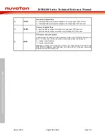
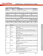
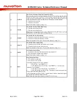
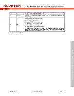
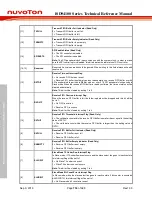
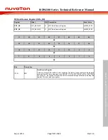
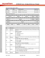
HALFDPX
SPI Half-duplex Transfer Enable Bit
This bit is used to select full-duplex or half-duplex for SPI transfer. The bit field DATDIR
(SPIn_CTL[20]) can be used to set the data direction in half-duplex transfer.
0 = SPI operates in full-duplex transfer.
1 = SPI operates in half-duplex transfer.
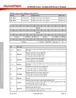
[13]
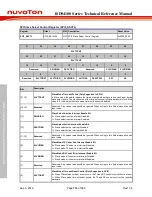
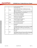
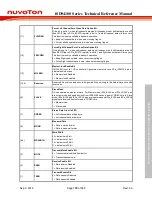
LSB
Send LSB First
0 = The MSB, which bit of transmit/receive register depends on the setting of DWIDTH, is
transmitted/received first.
1 = The LSB, bit 0 of the SPI TX register, is sent first to the SPI data output pin, and the first
bit received from the SPI data input pin will be put in the LSB position of the RX register (bit
0 of SPIn_RX).
[12:8]
DWIDTH
Data Width
This field specifies how many bits can be transmitted / received in one transaction. The
minimum bit length is 8 bits and can up to 32 bits.
DWIDTH = 0x08 …. 8 bits.
DWIDTH = 0x09 …. 9 bits.
……
DWIDTH = 0x1F …. 31 bits.
DWIDTH = 0x00 …. 32 bits.
Note:
For SPI1~SPI2, this bit field will decide the depth of TX/RX FIFO configuration in SPI
mode
.
Therefore, changing this bit field will clear TX/RX FIFO by hardware automatically in
SPI1~SPI2.
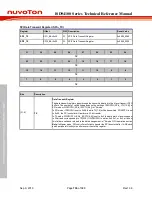
[7:4]
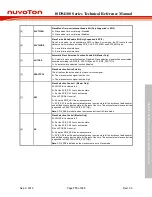
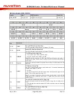
SUSPITV
Suspend Interval (Master Only)
The four bits provide configurable suspend interval between two successive transmit/receive
transaction in a transfer. The definition of the suspend interval is the interval between the
last clock edge of the preceding transaction word and the first clock edge of the following
transaction word. The default value is 0x3. The period of the suspend interval is obtained
according to the following equation.
(SUSPITV[3:0] + 0.5) * period of SPICLK clock cycle
Example:
SUSPITV = 0x0 …. 0.5 SPICLK clock cycle.
SUSPITV = 0x1 …. 1.5 SPICLK clock cycle.
……
SUSPITV = 0xE …. 14.5 SPICLK clock cycle.
SUSPITV = 0xF …. 15.5 SPICLK clock cycle.
[3]
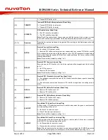
CLKPOL
Clock Polarity
0 = SPI bus clock is idle low.
1 = SPI bus clock is idle high.
[2]
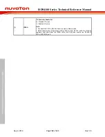
TXNEG
Transmit on Negative Edge
0 = Transmitted data output signal is changed on the rising edge of SPI bus clock.
1 = Transmitted data output signal is changed on the falling edge of SPI bus clock.
[1]
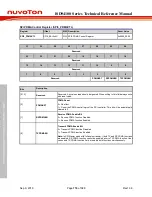
RXNEG
Receive on Negative Edge
0 = Received data input signal is latched on the rising edge of SPI bus clock.
1 = Received data input signal is latched on the falling edge of SPI bus clock.
Содержание ISD94100 Series
Страница 528: ...ISD94100 Series Technical Reference Manual Sep 9 2019 Page 528 of 928 Rev1 09 ISD94100 SERIES TECHNICAL REFERENCE MANUAL...
Страница 626: ...ISD94100 Series Technical Reference Manual Sep 9 2019 Page 626 of 928 Rev1 09 ISD94100 SERIES TECHNICAL REFERENCE MANUAL...
Страница 702: ...ISD94100 Series Technical Reference Manual Sep 9 2019 Page 702 of 928 Rev1 09 ISD94100 SERIES TECHNICAL REFERENCE MANUAL...
Страница 875: ...ISD94100 Series Technical Reference Manual Sep 9 2019 Page 875 of 928 Rev1 09 ISD94100 SERIES TECHNICAL REFERENCE MANUAL...


