ISD94100 Series Technical Reference Manual
Sep 9, 2019
Page
150
of 928
Rev1.09
IS
D
9
410
0
S
ER
IE
S
T
E
C
HN
ICA
L
RE
F
E
RE
NCE
M
AN
U
AL
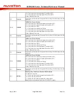
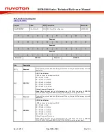
1 = Chip enters Power-down mode when the both PDWTCPU and PDEN bits are set to 1
and CPU runs WFI instruction.
Note:
This bit is write protected. Refer to the SYS_REGLCTL register.
[7]
PDEN
System Power-down Enable (Write Protected)
When this bit is set to 1, Power-down mode is enabled and chip
keeps active till the CPU sleep mode is also active and then the chip enters Power-down
mode.
When chip wakes up from Power-down mode, this bit is auto cleared. Users need to set this
bit again for next Power-down.
In Power-down mode, HXT and the HIRC will be disabled in this mode, but LXT and LIRC
are not controlled by Power-down mode.
In Power-down mode, the PLL and system clock are disabled, and ignored the clock source
selection. The clocks of peripheral are not controlled by Power-down mode, if the peripheral
clock source is from LXT or LIRC.
0 = Chip will not enter Power-down mode after CPU sleep command WFI.
1 = Chip enters Power-down mode after CPU sleep command WFI.
Note:
This bit is write protected. Refer to the SYS_REGLCTL register.
[6]
PDWKIF
Power-down Mode Wake-up Interrupt Status
Set by “Power-down wake-up event”, it indicates that resume from Power-down mode”
The flag is set if any wake-up source is occurred. Refer Power Modes and Wake-up Sources
chapter.
Note1:
Write 1 to clear the bit to 0.
Note2:
This bit works only if PDWKIEN (CLK_PWRCTL[5]) set to 1.
[5]
PDWKIEN
Power-down Mode Wake-up Interrupt Enable Bit (Write Protected)
0 = Power-down mode wake-up interrupt Disabled.
1 = Power-down mode wake-up interrupt Enabled.
Note1:
The interrupt will occur when both PDWKIF and PDWKIEN are high.
Note2:
This bit is write protected. Refer to the SYS_REGLCTL register.
[4]
PDWKDLY
Enable the Wake-up Delay Counter (Write Protected)
When the chip wakes up from Power-down mode, the clock control will delay certain clock
cycles to wait system clock stable.
The delayed clock cycle is 4096 clock cycles when chip works at external high speed crystal
oscillator (HXT), and 128 clock cycles when chip works at internal high speed RC oscillator
(HIRC).
0 = Clock cycles delay Disabled.
1 = Clock cycles delay Enabled.
Note:
This bit is write protected. Refer to the SYS_REGLCTL register.
[3]
LIRCEN
LIRC Enable Bit (Write Protected)
0 = Internal low speed RC oscillator (LIRC) Disabled.
1 = Internal low speed RC oscillator (LIRC) Enabled.
Note 1:
This bit is write protected. Refer to the SYS_REGLCTL register.
Note 2:
The reset value of this bit is 1.
Note 3:
The value of this bit must be kept 1.
[2]
HIRCEN
HIRC Enable Bit (Write Protected)
0 = Internal high speed RC oscillator (HIRC) Disabled.
1 = Internal high speed RC oscillator (HIRC) Enabled.
Note 1:
This bit is write protected. Refer to the SYS_REGLCTL register.
Note 2:
The reset value of this bit is 1.
Содержание ISD94100 Series
Страница 528: ...ISD94100 Series Technical Reference Manual Sep 9 2019 Page 528 of 928 Rev1 09 ISD94100 SERIES TECHNICAL REFERENCE MANUAL...
Страница 626: ...ISD94100 Series Technical Reference Manual Sep 9 2019 Page 626 of 928 Rev1 09 ISD94100 SERIES TECHNICAL REFERENCE MANUAL...
Страница 702: ...ISD94100 Series Technical Reference Manual Sep 9 2019 Page 702 of 928 Rev1 09 ISD94100 SERIES TECHNICAL REFERENCE MANUAL...
Страница 875: ...ISD94100 Series Technical Reference Manual Sep 9 2019 Page 875 of 928 Rev1 09 ISD94100 SERIES TECHNICAL REFERENCE MANUAL...


