


522
Bit 0
Bit 1
Bit 2
Bit 3
Bit 4
Bit 5
Bit 6
Bit 7
LSB
MSB
Synchroni-
zation clock
Serial data
*
*
Transfer direction
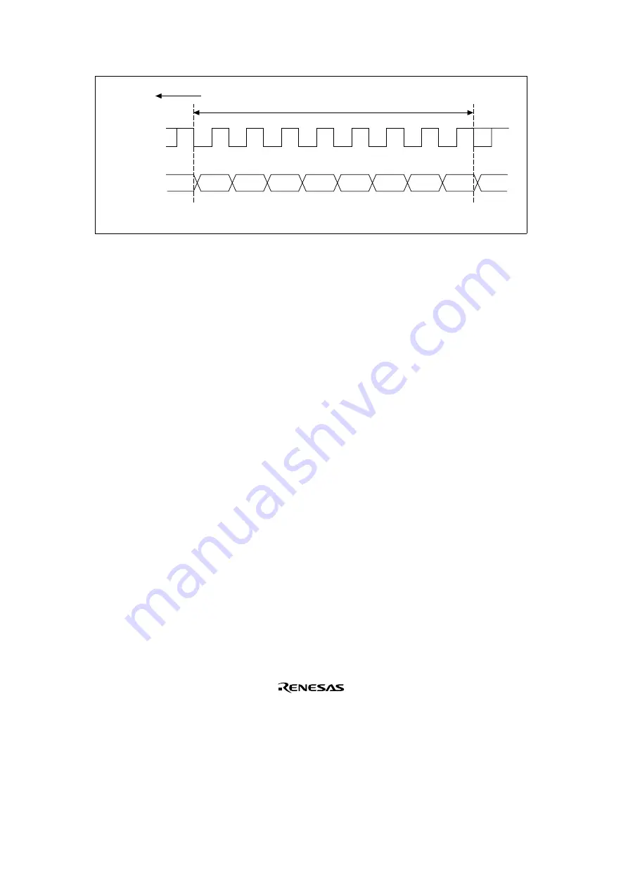
One unit (character or frame) of communication data
Note:
*
High except in continuous transmitting or receiving.
Figure 14.16 Data Format in Clock Synchronous Communication
In clock synchronous serial communication, each data bit is output on the communication line
from one falling edge of the serial clock to the next. Data are guaranteed valid at the rising edge of
the serial clock. In each character, the serial data bits are transmitted in order from the LSB (first)
to the MSB (last). After output of the MSB, the communication line remains in the state of the
MSB. In the clock synchronous mode, the SCI transmits or receives data by synchronizing with
the falling edge of the synchronization clock.
Communication Format: The data length is fixed at eight bits. No parity bit or multiprocessor bit
can be added.
Clock: An internal clock generated by the on-chip baud rate generator or an external clock input
from the SCK pin can be selected as the SCI transmit/receive clock. The clock source is selected
by the C/
A
bit in the serial mode register (SMR) and bits CKE1 and CKE0 in the serial control
register (SCR). See table 14.9.
When the SCI operates on an internal clock, it outputs the clock signal at the SCK pin. Eight clock
pulses are output per transmitted or received character. When the SCI is not transmitting or
receiving, the clock signal remains in the high state.
Note:
An overrun error occurs only during the receive operation, and the sync clock is output
until the RE bit is cleared to 0. When you want to perform a receive operation in one-
character units, select external clock for the clock source.
SCI Initialization (Clock Synchronous Mode): Before transmitting or receiving, software must
clear the TE and RE bits to 0 in the serial control register (SCR), then initialize the SCI as follows.
When changing the mode or communication format, always clear the TE and RE bits to 0 before
following the procedure given below. Clearing TE to 0 sets TDRE to 1 and initializes the transmit
shift register (TSR). Clearing RE to 0, however, does not initialize the RDRF, PER, FER, and
ORER flags and receive data register (RDR), which retain their previous contents.
Summary of Contents for SH7041 Series
Page 2: ......
Page 6: ......
Page 38: ...xvi ...
Page 44: ...6 ...
Page 46: ...8 ...
Page 48: ...10 ...
Page 82: ...44 ...
Page 114: ...76 ...
Page 118: ...80 ...
Page 124: ...86 ...
Page 170: ...132 ...
Page 250: ...212 ...
Page 492: ...454 ...
Page 506: ...468 ...
Page 604: ...566 ...
Page 684: ...646 ...
Page 706: ...668 ...
Page 778: ...740 ...
Page 780: ...742 ...
Page 818: ...780 ...
Page 850: ...812 ...
Page 923: ...SH7040 SH7041 SH7042 SH7043 SH7044 SH7045 Group Hardware Manual REJ09B0044 0600O ...