
Chapter 2. Signal Descriptions and Clocking
2-31
Detailed Signal Descriptions
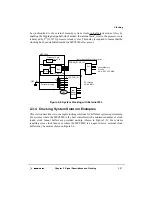
2.2.5.10.4 Memory Interface Valid (MIV)—Output
The MIV signal is intended to help reduce the number of bus cycles that logic analyzers
must store in memory during a debug trace by signalling when address and data signals
should be sampled.
State Meaning
Asserted—The memory interface valid signal, MIV, is asserted
whenever FPM, EDO, SDRAM, Flash, or ROM addresses or data are
present on the external memory bus.
Timing Comments
Assertion/Negation—Section 15.4.1, “MIV Signal
Timing,”describes the relative timing of MIV in detail.
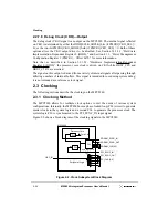
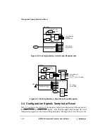
2.2.6 Test and Configuration Signals
The MPC8240 has several signals that are sampled during reset to determine the
configuration of the ROM, Flash, and dynamic memory, and the phase-locked loop clock
mode.
To facilitate system testing, the MPC8240 provides a JTAG test access port (TAP) that
complies with the IEEE 1149.1 boundary-scan specification. This section also describes the
JTAG test access port signals.
2.2.6.1 PLL Configuration (PLL_CFG[0:4])—Input
PLL_CFG[0:4] determine the clock frequency relationships of the PCI clock, the processor
core frequency, and the sys_logic_clk signal (that determines the frequency of the memory
interface clock). The multiplier factor determined by these signals on reset is stored in
HID1[PLLRATIO]. However, system software cannot read the PLLRATIO value and
associate it with a unique PLL_CFG[0:4] value. See Section 5.3.1.2.2, “Hardware
Implementation-Dependent Register 1 (HID1),” for more information on HID1.
State Meaning
Asserted—See the MPC8240 Hardware Specification for the
supported settings.
Timing Comments
Assertion—These signals are sampled at the negation of
HRST_CPU and HRST_CTRL as part of the reset configuration
signals. See Section 2.4, “Configuration Signals Sampled at Reset.”
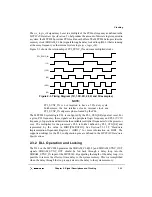
2.2.6.2 JTAG Test Clock (TCK)—Input
The JTAG test clock (TCK) signal is an input on the MPC8240. Following is the state
meaning for the TCK input signal.
State Meaning
Asserted/Negated—This input should be driven by a free-running
clock signal with a 30–70% duty cycle. Input signals to the test
access port are clocked in on the rising edge of TCK. Changes to the
test access port output signals occur on the falling edge of TCK. The
test logic allows TCK to be stopped.
Note that this input contains an internal pull-up resistor to ensure that
an unterminated input appears as a high signal level to the test logic.
Содержание MPC8240
Страница 1: ...MPC8240UM D Rev 1 1 2001 MPC8240 Integrated Processor User s Manual ...
Страница 38: ...xviii MPC8240 Integrated Processor User s Manual TABLES Table Number Title Page Number ...
Страница 48: ...xlviii MPC8240 Integrated Processor User s Manual Acronyms and Abbreviations ...
Страница 312: ...6 94 MPC8240 Integrated Processor User s Manual ROM Flash Interface Operation ...
Страница 348: ...7 36 MPC8240 Integrated Processor User s Manual PCI Host and Agent Modes ...
Страница 372: ...8 24 MPC8240 Integrated Processor User s Manual DMA Register Descriptions ...
Страница 394: ...9 22 MPC8240 Integrated Processor User s Manual I2O Interface ...
Страница 412: ...10 18 MPC8240 Integrated Processor User s Manual Programming Guidelines ...
Страница 454: ...12 14 MPC8240 Integrated Processor User s Manual Internal Arbitration ...
Страница 466: ...13 12 MPC8240 Integrated Processor User s Manual Exception Latencies ...
Страница 516: ...16 14 Watchpoint Trigger Applications ...
Страница 538: ...B 16 MPC8240 Integrated Processor User s Manual Setting the Endian Mode of Operation ...
Страница 546: ...C 8 MPC8240 Integrated Processor User s Manual ...
Страница 640: ...INDEX Index 16 MPC8240 Integrated Processor User s Manual ...


