4-18
MPC8240 Integrated Processor User’s Manual
Peripheral Logic Power Management Configuration Registers (PMCRs)
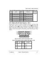
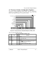
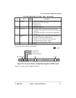
4.3.2 Power Management Configuration Register 2
(PMCR2)—Offset 0x72
Power management configuration register 2 (PMCR2), shown in Figure 4-6, is a 1-byte
register located at offset 0x72.
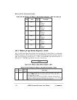
11–8
—
0
Reserved
7
PM
0
Power management enable
0 Disables the peripheral logic power management logic within the MPC8240
1 Enables the peripheral logic power management logic within the MPC8240
6
—
0
Reserved
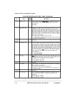
5
DOZE
0
Enables/disables the doze mode capability of the MPC8240. Note that this bit is
only valid if MPC8240 power management is enabled.
(PMCR1[PM] = 1).
0 Disables the doze mode
1 Enables the doze mode
4
NAP
0
Enables/disables the nap mode capability of the MPC8240. Note that this bit is
only valid if MPC8240 power management is enabled.
(PMCR1[PM] = 1).
0 Disables the nap mode
1 Enables the nap mode
3
SLEEP
0
Enables/disables the sleep mode capability of the MPC8240. Note that this bit
is only valid if MPC8240 power management is enabled
(PMCR1[PM] = 1).
0 Disables the sleep mode
1 Enables the sleep mode
2–1
CKO_MODE
00
Selects the clock source for the test clock output when CKO_SEL = 1.
00 Disables the test clock output driver
01 Selects the internal sys_logic_clk signal as the test clock output source
10 Selects one-half of the PCI rate clock as the test clock output source
11 Selects the internal PCI rate clock as the test clock output source
0
CKO_SEL
x
The initial value of this bit is determined by the AS reset configuration bit, which
selects either the clock output of the processor core or the clock output of the
system logic to be driven out of the CKO signal.
0 Processor core clock selected. The signal driven by CKO is determined by
HID0[ECLK,SBCLK]. See Section 5.3.1.2.1, “Hardware
Implementation-Dependent Register 0 (HID0),” for the available choices.
1 System logic clock selected. The signal driven by CKO is determined by the
encoding of the CKO_MODE bits above. See CKO_MODE field description
for the available choices.
Table 4-15. Bit Settings for Power Management Configuration
Register 1—0x70 (Continued)
Bits
Name
Reset
Value
Description
Содержание MPC8240
Страница 1: ...MPC8240UM D Rev 1 1 2001 MPC8240 Integrated Processor User s Manual ...
Страница 38: ...xviii MPC8240 Integrated Processor User s Manual TABLES Table Number Title Page Number ...
Страница 48: ...xlviii MPC8240 Integrated Processor User s Manual Acronyms and Abbreviations ...
Страница 312: ...6 94 MPC8240 Integrated Processor User s Manual ROM Flash Interface Operation ...
Страница 348: ...7 36 MPC8240 Integrated Processor User s Manual PCI Host and Agent Modes ...
Страница 372: ...8 24 MPC8240 Integrated Processor User s Manual DMA Register Descriptions ...
Страница 394: ...9 22 MPC8240 Integrated Processor User s Manual I2O Interface ...
Страница 412: ...10 18 MPC8240 Integrated Processor User s Manual Programming Guidelines ...
Страница 454: ...12 14 MPC8240 Integrated Processor User s Manual Internal Arbitration ...
Страница 466: ...13 12 MPC8240 Integrated Processor User s Manual Exception Latencies ...
Страница 516: ...16 14 Watchpoint Trigger Applications ...
Страница 538: ...B 16 MPC8240 Integrated Processor User s Manual Setting the Endian Mode of Operation ...
Страница 546: ...C 8 MPC8240 Integrated Processor User s Manual ...
Страница 640: ...INDEX Index 16 MPC8240 Integrated Processor User s Manual ...


