


Appendix E. Processor Core Register Summary
E-13
PowerPC Register Set
•
Miscellaneous registers
— The time base facility (TB) for writing. The TB is a 64-bit register pair that can
be used to provide time of day or interval timing. It consists of two 32-bit
registers—time base upper (TBU) and time base lower (TBL). The TB is
incremented once every four sys_logic_clk cycles.
— Decrementer (DEC). The DEC register is a 32-bit decrementing counter that
provides a mechanism for causing a decrementer exception after a
programmable delay. The DEC is decremented once every four sys_logic_clk
cycles.
— External access register (EAR). This optional register is used in conjunction with
the eciwx and ecowx instructions. While the PowerPC architecture specifies that
the low-order six bits of the EAR (bits 26–31) are used to select a device, the
603e and MPC8240 only implement the low-order 4 bits (bits 28–31). Note that
the EAR register and the eciwx and ecowx instructions are optional in the
PowerPC architecture and may not be supported in all PowerPC processors that
implement the OEA.
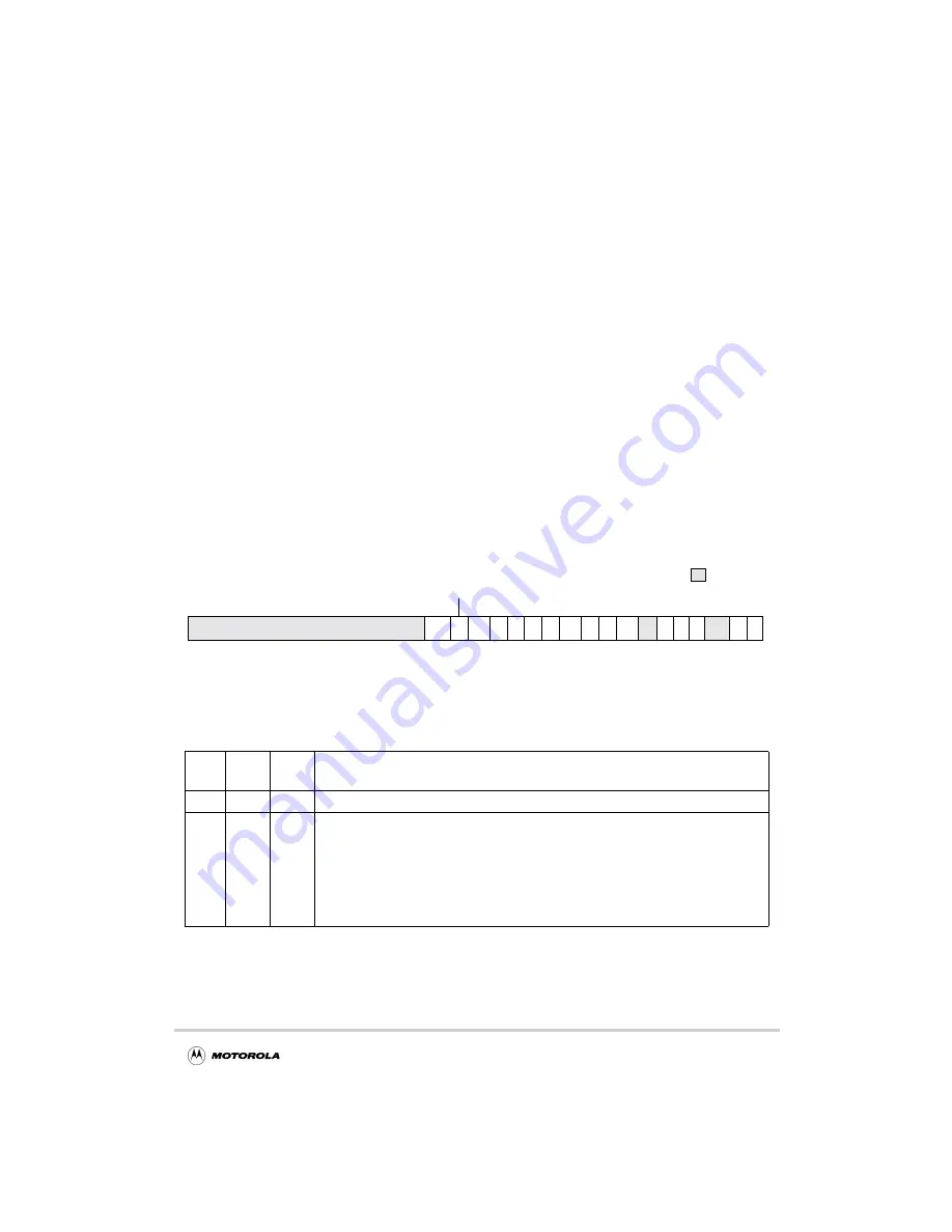
E.1.3.1 Machine State Register (MSR)
The machine state register (MSR) is shown in Figure E-10.
Figure E-10. Machine State Register (MSR)
Table E-8 shows the bit definitions for the MSR.
Table E-8. MSR Bit Settings
Bit(s)
Name
Reset
Value
Description
0–12
—
0
Reserved
13
POW
0
Power management enable (603e-specific)
0 Power management disabled (normal operation mode)
1 Power management modes enabled (doze, nap, or sleep mode)
This bit controls the programmable power modes only; it has no effect on dynamic power
management (DPM). MSR[POW] may be altered with an mtmsr instruction only. Also,
when altering the POW bit, software may alter only this bit in the MSR and no others with
the same instruction. The mtmsr instruction must be followed by a context-synchronizing
instruction.
0
12
13
14 15 16 17 18 19 20 21 22 23
24 25 26 27 28 29 30 31
Reserved
0000 0000 0000 0
POW
ILE EE PR FP ME FE0 SE BE FE1 0
IP IR DR 00
RI LE
TGPR
Содержание MPC8240
Страница 1: ...MPC8240UM D Rev 1 1 2001 MPC8240 Integrated Processor User s Manual ...
Страница 38: ...xviii MPC8240 Integrated Processor User s Manual TABLES Table Number Title Page Number ...
Страница 48: ...xlviii MPC8240 Integrated Processor User s Manual Acronyms and Abbreviations ...
Страница 312: ...6 94 MPC8240 Integrated Processor User s Manual ROM Flash Interface Operation ...
Страница 348: ...7 36 MPC8240 Integrated Processor User s Manual PCI Host and Agent Modes ...
Страница 372: ...8 24 MPC8240 Integrated Processor User s Manual DMA Register Descriptions ...
Страница 394: ...9 22 MPC8240 Integrated Processor User s Manual I2O Interface ...
Страница 412: ...10 18 MPC8240 Integrated Processor User s Manual Programming Guidelines ...
Страница 454: ...12 14 MPC8240 Integrated Processor User s Manual Internal Arbitration ...
Страница 466: ...13 12 MPC8240 Integrated Processor User s Manual Exception Latencies ...
Страница 516: ...16 14 Watchpoint Trigger Applications ...
Страница 538: ...B 16 MPC8240 Integrated Processor User s Manual Setting the Endian Mode of Operation ...
Страница 546: ...C 8 MPC8240 Integrated Processor User s Manual ...
Страница 640: ...INDEX Index 16 MPC8240 Integrated Processor User s Manual ...


