


6-46
MPC8240 Integrated Processor User’s Manual
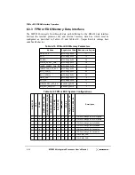
FPM or EDO DRAM Interface Operation
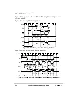
6.3 FPM or EDO DRAM Interface Operation
Figure 6-29 shows an internal block diagram of the FPM and EDO DRAM interface for the
MPC8240.
Figure 6-29. FPM or EDO DRAM Memory Interface Block Diagram
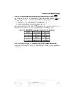
The MPC8240 supports a variety of DRAM configurations, through SIMM, DIMM, or
direct board attachment. Thirteen address pins provide for DRAM device densities of up to
64 Mbits. Eight row address strobe (RAS) signals support up to eight banks of memory.
Each bank can be 8 bytes wide; eight column address strobe (CAS) signals are used to
provide byte selection for writes. The banks can be built of DRAMs, SIMMs or DIMMs
that range from 4 to 128 Mbits as described in Table 6-17. The memory design must be
byte-selectable for writes using CAS. The MPC8240 allows up to 1 Gbyte of addressable
memory.
In addition to the CAS[0:7] signals, RAS[0:7] signals, and address signals SDMA[12:0]
and SDBA[1:0], there are 64 data signals MDH[0:31] and MDL[0:31], a write enable (WE)
signal, and one parity bit per byte-width of data PAR[0:7] for a total of 102 DRAM memory
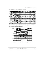
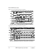
signals. Figure 6-30 is an example of a two-bank 16-Mbyte DRAM system. Figure 6-31
shows an example DRAM organization.
DRAM
ECC
DRAM
Address
Address
(Processor or PCI)
DRAM Memory Control
Processor data to DRAM
Processor data from DRAM
DRAM write output enable
Central Control Unit
FPM or EDO DRAM Memory Interface
SDMA[12:0]
RAS[0:7]
CAS[0:7]
PAR[0:7]
DRAM Memory Array
Data
MDH[0:31]
MDL[0:31]
Control
MUX
Row
Col
Note: selectable
Flow Through Buffering
Error Checking
•64-bit ECC (No In-line ECC)
•Parity
Содержание MPC8240
Страница 1: ...MPC8240UM D Rev 1 1 2001 MPC8240 Integrated Processor User s Manual ...
Страница 38: ...xviii MPC8240 Integrated Processor User s Manual TABLES Table Number Title Page Number ...
Страница 48: ...xlviii MPC8240 Integrated Processor User s Manual Acronyms and Abbreviations ...
Страница 312: ...6 94 MPC8240 Integrated Processor User s Manual ROM Flash Interface Operation ...
Страница 348: ...7 36 MPC8240 Integrated Processor User s Manual PCI Host and Agent Modes ...
Страница 372: ...8 24 MPC8240 Integrated Processor User s Manual DMA Register Descriptions ...
Страница 394: ...9 22 MPC8240 Integrated Processor User s Manual I2O Interface ...
Страница 412: ...10 18 MPC8240 Integrated Processor User s Manual Programming Guidelines ...
Страница 454: ...12 14 MPC8240 Integrated Processor User s Manual Internal Arbitration ...
Страница 466: ...13 12 MPC8240 Integrated Processor User s Manual Exception Latencies ...
Страница 516: ...16 14 Watchpoint Trigger Applications ...
Страница 538: ...B 16 MPC8240 Integrated Processor User s Manual Setting the Endian Mode of Operation ...
Страница 546: ...C 8 MPC8240 Integrated Processor User s Manual ...
Страница 640: ...INDEX Index 16 MPC8240 Integrated Processor User s Manual ...


