


7-24
MPC8240 Integrated Processor User’s Manual
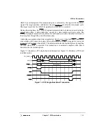
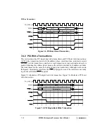
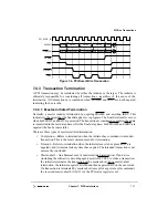
PCI Bus Transactions
address in the range from 0xFEC0_0000 to 0xFEDF_FFFF for the CONFIG_ADDR
register, the address 0xFEC0_0CF8 may be the most intuitive location. For address map A,
the processor core can access the CONFIG_ADDR register through the MPC8240 at
0x8000_0CF8. See Appendix A for more information on address map A.
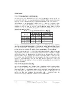
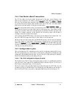
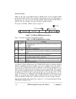
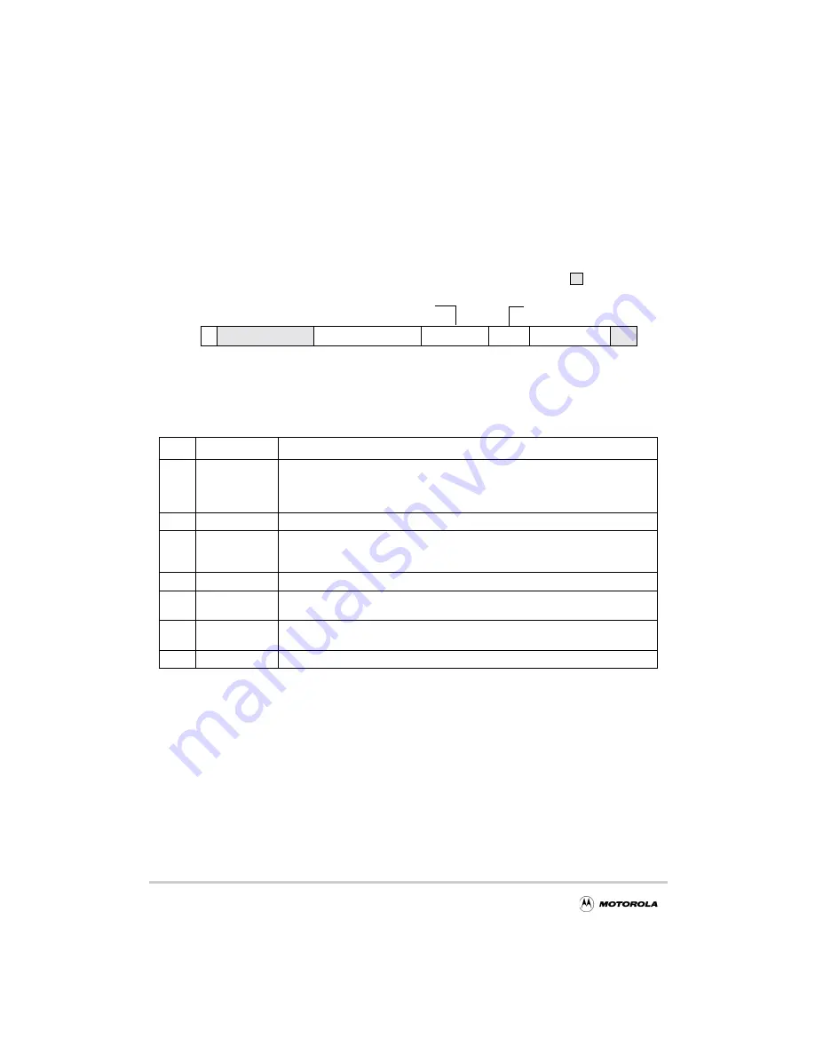
The format of CONFIG_ADDR is shown in Figure 7-9.
Figure 7-9. CONFIG_ADDR Register Format
Table 7-5 describes the fields within CONFIG_ADDR.
As with the CONFIG_ADDR register, the CONFIG_DATA register is located at different
addresses depending on the memory address map in use. For address map A, the processor
can access the CONFIG_DATA register through the MPC8240 at 0x8000_0CFC to
0x8000_0CFF. For address map B, the processor can access the CONFIG_DATA register
at any location in the address range from 0xFEE0_0000 to 0xFEEF_FFFF. For simplicity,
the address for CONFIG_DATA is sometimes referred to as CFC, 0xnnnn_nCFC or CFCh
(in the PCI literature as). Although systems implementing address map B can use any
address in the range from 0xFEE0_0000 to 0xFEEF_FFFF for the CONFIG_DATA
register, the address 0xFEE0_0CFC–0xFEE0_0CFF may be the most intuitive location.
Note that the CONFIG_DATA register may contain 1, 2, 3, or 4 bytes depending on the size
of the register being accessed.
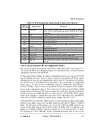
Table 7-5. CONFIG_ADDR Register Fields
Bits
Field Name
Description
31
E(nable)
The enable flag controls whether accesses to CONFIG_DATA are translated into PCI
configuration cycles.
1 Enabled
0 Disabled
30–24
—
Reserved (must be 0b000_0000)
23–16
Bus number
This field is an encoded value used to select the target bus of the configuration access.
For target devices on the PCI bus connected to the MPC8240, this field should be set to
0x00.
15–11
Device number
This field is used to select a specific device on the target bus.
10–8
Function number
This field is used to select a specific function in the requested device. Single-function
devices should respond to function number 0b000.
7–2
Register number
This field is used to select the address offset in the configuration space of the target
device.
1–0
—
Reserved (must be 0b00)
E
0 0 0 0 0 0 0
Bus Number
Register Number
0 0
31
30
24 23
16 15
11 10
8
7
2
1
0
Reserved
Function Number
Device Number
Содержание MPC8240
Страница 1: ...MPC8240UM D Rev 1 1 2001 MPC8240 Integrated Processor User s Manual ...
Страница 38: ...xviii MPC8240 Integrated Processor User s Manual TABLES Table Number Title Page Number ...
Страница 48: ...xlviii MPC8240 Integrated Processor User s Manual Acronyms and Abbreviations ...
Страница 312: ...6 94 MPC8240 Integrated Processor User s Manual ROM Flash Interface Operation ...
Страница 348: ...7 36 MPC8240 Integrated Processor User s Manual PCI Host and Agent Modes ...
Страница 372: ...8 24 MPC8240 Integrated Processor User s Manual DMA Register Descriptions ...
Страница 394: ...9 22 MPC8240 Integrated Processor User s Manual I2O Interface ...
Страница 412: ...10 18 MPC8240 Integrated Processor User s Manual Programming Guidelines ...
Страница 454: ...12 14 MPC8240 Integrated Processor User s Manual Internal Arbitration ...
Страница 466: ...13 12 MPC8240 Integrated Processor User s Manual Exception Latencies ...
Страница 516: ...16 14 Watchpoint Trigger Applications ...
Страница 538: ...B 16 MPC8240 Integrated Processor User s Manual Setting the Endian Mode of Operation ...
Страница 546: ...C 8 MPC8240 Integrated Processor User s Manual ...
Страница 640: ...INDEX Index 16 MPC8240 Integrated Processor User s Manual ...


