6-50
MPC8240 Integrated Processor User’s Manual
FPM or EDO DRAM Interface Operation
6.3.2 FPM or EDO DRAM Address Multiplexing
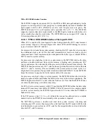
System software must configure the MPC8240 at reset to appropriately multiplex the row
and column address bits for each bank. This is done by writing the row address
configuration into the memory control configuration register 1 (MCCR1); see Section 4.10,
“Memory Control Configuration Registers.”
The internal physical addresses A[0
msb
:31
lsb
] is multiplexed through the output address
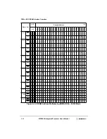
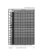
pins SDMA[12:0]. The row and column bit configuration settings are shown in Figure 6-32
for 32-bit bus mode and Figure 6-33 for 64-bit bus mode. During the RAS and CAS phases,
the unshaded row and column bits SDMA[12:0] multiplex the appropriate physical
addresses.
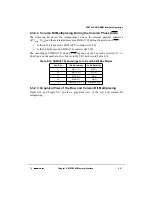
6.3.2.1 Row Bit Multiplexing During The Row Phase (RAS)
The following list shows the relationships between the internal physical addresses
A[5
msb
– 20
lsb
] and the external address pins SDMA[12:0] during the assertion of RAS:
•
In the 32-bit data bus mode, SDMA12 contains A[6].
•
In the 64-bit data bus mode SDMA12 contains A[5].
•
If the FPM or EDO has 9 row bits, SDMA[8:0] contains A[12:20].
•
If the FPM or EDO has 10 row bits, SDMA[9:0] contains A[11:20].
•
If the FPM or EDO has 11 row bits, SDMA[10:0] contains A[10:20].
•
If the FPM or EDO has 12 or 13 row bits, SDMA[11:0] contains A[9:20].
Note that SDMA12 is only used as the most-significant row address bit for 13 x 11
FPM or EDO arrays.
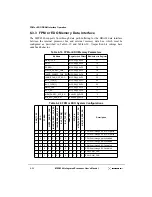
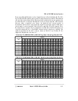
64 Mbits
2
2 Mbits x 32
12 x 9
16
128
2
2 Mbits x 32
11 x 10
16
128
4
4 Mbits x 16
12 x 10
32
256
4
4 Mbits x 16
11 x 11
32
256
8
8 Mbits x 8
12 x 11
64
512
16
16 Mbits x 4
13 x 11
128
1024
16
16 Mbits x 4
12 x 12
128
1024
Table 6-17. Supported FPM or EDO DRAM Device Configurations (Continued)
DRAM
Devices
Devices
(64-bit
Bank)
Device
Configuration
Row x Column
Bits
64-bit
Bank Size
(Mbytes)
8 Banks of
Memory
(Mbytes)
Содержание MPC8240
Страница 1: ...MPC8240UM D Rev 1 1 2001 MPC8240 Integrated Processor User s Manual ...
Страница 38: ...xviii MPC8240 Integrated Processor User s Manual TABLES Table Number Title Page Number ...
Страница 48: ...xlviii MPC8240 Integrated Processor User s Manual Acronyms and Abbreviations ...
Страница 312: ...6 94 MPC8240 Integrated Processor User s Manual ROM Flash Interface Operation ...
Страница 348: ...7 36 MPC8240 Integrated Processor User s Manual PCI Host and Agent Modes ...
Страница 372: ...8 24 MPC8240 Integrated Processor User s Manual DMA Register Descriptions ...
Страница 394: ...9 22 MPC8240 Integrated Processor User s Manual I2O Interface ...
Страница 412: ...10 18 MPC8240 Integrated Processor User s Manual Programming Guidelines ...
Страница 454: ...12 14 MPC8240 Integrated Processor User s Manual Internal Arbitration ...
Страница 466: ...13 12 MPC8240 Integrated Processor User s Manual Exception Latencies ...
Страница 516: ...16 14 Watchpoint Trigger Applications ...
Страница 538: ...B 16 MPC8240 Integrated Processor User s Manual Setting the Endian Mode of Operation ...
Страница 546: ...C 8 MPC8240 Integrated Processor User s Manual ...
Страница 640: ...INDEX Index 16 MPC8240 Integrated Processor User s Manual ...


