Serial Peripheral Interface Controller
UG0331 User Guide Revision 15.0
505
14.2
Functional Description
This section provides the detailed description of SPI peripherals.
14.2.1
Architecture Overview
The SPI controller supports master and slave modes of an operation.
•
In master mode, the SPI generates SPI_X_CLK, selects a slave using SPI_X_SS[x], transmits the
data on SPI_X_DO, and receives the data on SPI_X_DI.
•
In slave mode, the SPI is selected by SPI_X_SS[0]. The SPI receives a clock on SPI_X_CLK and
incoming data on SPI_X_DI.
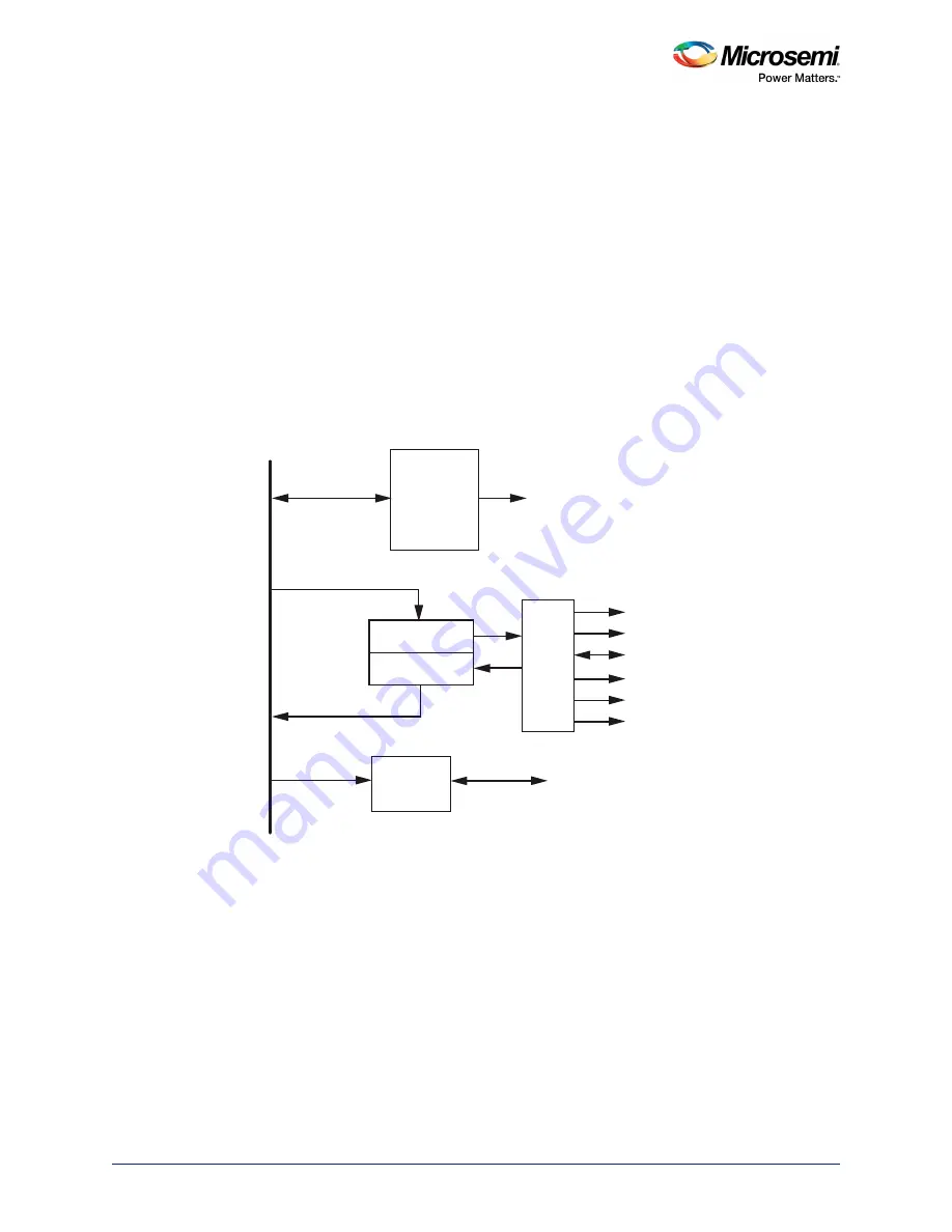
The SPI peripherals consist mainly of the following components (refer
•
Transmit and receive FIFOs
•
Configuration and control logic
•
SPI clock generator
The following figure shows the SPI controller block diagram.
Figure 205 •
SPI Controller Block Diagram
Note:
X is used as a place holder for 0 or 1 in the register and signal descriptions. It indicates SPI _0 (on the
APB_0 bus) or SPI_1 (on the APB_1 bus).
14.2.1.1 Transmit and Receive FIFOs
The SPI controller embeds two 4 × 32 (depth × width) FIFOs for receive and transmit, as shown in
page 505. These FIFOs are accessible through RX data and TX data registers (refer to the
page 528). Writing to the TX data register causes the data to be written to the
transmit FIFO. This is emptied by the transmit logic. Similarly, reading from the RX data register causes
the data to be read from the receive FIFO. The not-empty port of the receive FIFO and the not-full port of
the transmit FIFO flags (of the FIFOs) are exposed as SPI_X_RXAVAIL (SPI has data to be read) and
&RQILJXUDWLRQ
DQG
&RQWUROORJLF
63,B;B,17
$3%%XV
3:'$7$>@
35'$7$>@
;7UDQVPLW),)2
;5HFHLYH),)2
7;5;
/RJLF
63,B;B'2
63,B;B',
63,B;B66
63,B;B7;5)0
63,B;B5;$9$,/
63,B;B'2(B1
63,B;B&/.
63,&ORFN
*HQHUDWRU
$3%B;B&/.
1RWH
7KH63,B;B'263,B;B',63,B;B66DQG63,B;B&/.VLJQDOVDUHDYDLODEOH
WRWKH)3*$IDEULF
63,B;B'2(B1LVDFFHVVLEOHWKURXJKWKH63,FRQWUROUHJLVWHU
63,B;B7;5)0DQG63,B;B5;$9$,/VLJQDOVDUHXVHGRQO\E\3'0$
63,B;B,17LVVHQWWRWKH&RUWH[0SURFHVVRU


