Cache Controller
UG0331 User Guide Revision 15.0
144
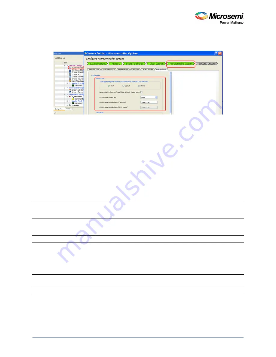
The selection of the main memory for the Cache Controller can also be made using the system builder
flow of the Libero SoC software. This procedure is explained in the following figure.
Figure 64 •
System Builder with Remapping Options for eNVM, eSRAM, and MDDR
Cache Controller configurations like enable/disable, selecting the main memory, and Cache Locked
mode can also be performed using the firmware/application code with the register settings provided in
the
System Registers Used for Cache Operations,
Refer to the following application notes for more details on the Cache Controller configurations:
•
AC389: SmartFusion2 SoC FPGA - Cache Controller Configuration Application Note
•
AC390: SmartFusion2 SoC FPGA – Remapping eNVM, eSRAM, and DDR/SDR SDRAM Memories
Application Note
Note:
Create or modify the linker scripts/linker settings of the application in such a way that all read and write
data sections are in non-cacheable memory regions or accessed through the system bus address space.
This note has to be strictly followed if eSRAM or DDR SDRAM are selected as the main memory for the
cache.
4.3.1
System Registers Used for Cache Operations
Detailed bit-level descriptions of the cache registers are provided in the
Table 92 •
System Registers for Cache Operations
Register Name
Register
Type
Flash
Write
Protect
Reset Source
Description
RW-P
Register
SYSRESET_N Used to configure cache options like cache
enable/disable, cache lock enable/disable,
Debug mode system bus read & write.
RW-P
Register
SYSRESET_N Defines the cache region size
RW-P
Register
SYSRESET_N If Cache Lock mode is enabled and if there is
an ECC error while accessing the Cache
Memory, the base address can be used to
initiate the transaction to re-read the
erroneous data from the system memory
which is stored in this register.
RW-P
Register
SYSRESET_N Used when Cache Memory index is to be
flushed or invalidated.
RW
N/A
SYSRESET_N Used to flush the Cache Memory


