Serial Peripheral Interface Controller
UG0331 User Guide Revision 15.0
512
14.2.2.3.5 Devices Requiring Data Frame Sizes of More than 32 Bits
Serial flash devices such as the Atmel AT25DF321 which support mode 3 (SPO = 1 and SPH = 1)
require more than 32 bits of frame data in some modes. To drive these devices, continuous transfers are
required from the SPI interface while holding the slave select low continuously (which is connected to the
chip select of the target device). This is accomplished by using the transmit FIFO from the SPI, which
enforces continuous back-to-back transfers, if it is not empty. The slave select continues to be held low
(active) in SPI mode 3 (SPO = 1 and SPH = 1) and not pulsed between data frames.
For example, to send 64 bits to the AT25DF321 (8-bit opcode, 24-bit address, 4 data bytes), the data
frame size (
) can be set to 32 and the data frame count set to two
(
] field).
TXRXDFCOUNT Register
The SPI peripheral contains a TXRXDFCOUNT counter (found in the
number of transmitted and received frames. Its function varies in master and slave modes.
TXRXDFCOUNT in master mode controls the following:
•
The Tx and Rx done interrupts
•
Terminates the auto fill and empty operations
•
Holds slave select active
TXRXDFCOUNT in slave mode controls the following:
•
The Tx and Rx done interrupts
•
Terminates the auto fill operation
In slave operation, it is possible for TXRXDFCOUNT to miscount actual transmitted and received frames
if the transmit FIFO under-run condition occurs. If this is likely in an application, Microsemi recommends
that TXRXDFCOUNT not be used and that it be disabled. Instead use the CMDINT and SSEND bits in
the raw interrupt status (RIS) register to monitor operation, or simply count how many frames it is
received.
Page Program for Atmel AT25DF321
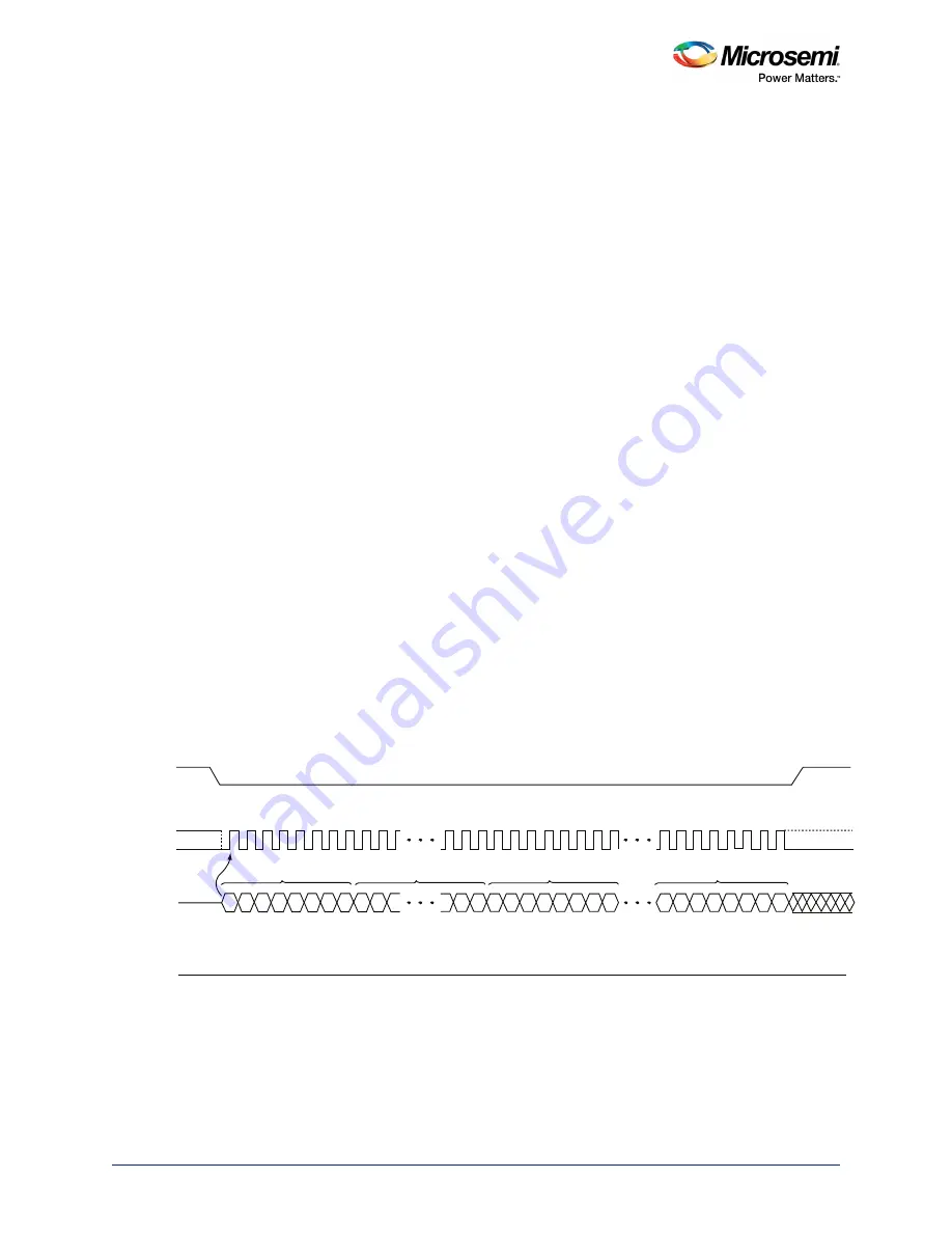
The following figure shows the Page Programming Timing for Atmel AT25DF321. In this mode, the
opcode, address, and data require more than 32 clock periods. To drive this device, the chip select (CS)
can be connected to the slave select signal, the data frame size set to 16, and the FIFO repeatedly filled
until the target flash device is programmed. As long as the data is available to transmit in the FIFO, the
chip select signal (connected to slave select on the SPI controller) will be asserted Low.
Figure 213 •
Page Program Timing
Devices That Do Not Support Mode 1 (SPO = 0 and SPH = 1) or Mode 3 (SPO = 1 and SPH = 1)
For flash devices that do not support mode 1 (SPO = 0 and SPH = 1) or mode 3 (SPO = 1 and SPH = 1),
it is necessary to use a dedicated GPIO pin to drive the chip select signal.
Data in Byte n
Data in Byte 1
Opcode
Address Bits A23-A0
MSB
MSB
MSB
MSB
High Impedance
0
0
0
0
0
0
0
0 A
D
A
D
A
D
A
D
A
D
A
D
D D
D D
D D
D D
D D
1
1
2
3
4
5
6
7
8
9
29 30 31 32 33 34 35
37 38 39
36
SPI_SS[x]
SPI_CLK
SPI_DO
SPI_DI


