


XC2200 Derivatives
System Units (Vol. 1 of 2)
System Control Unit (SCU)
User’s Manual
6-6
V2.1, 2008-08
SCU, V1.13
– Unlocked Mode
– Normal Mode
•
Different power saving modes
– Power Down
– Sleep Mode (VCO Power Down)
•
Glitchless programming of output divider K2 and VCO bypass divider K1
•
Glitchless switching between Normal Mode and Prescaler Mode
•
Trimmed current controlled clock source
6.1.4.2
PLL Functional Description
The PLL consists of a Voltage Controlled Oscillator (VCO) with a feedback path. A
divider in the feedback path (N-Divider) divides the VCO frequency. The resulting
frequency is then compared with the divided external frequency (P-Divider). The phase
detection logic determines the difference between the two clocks and accordingly
controls the frequency of the VCO (
f
VCO
). A PLL lock detection unit monitors and signals
this condition. The phase detection logic continues to monitor the two clocks and adjusts
the VCO clock if required. The PLL output clock
f
PLL
is derived from the VCO clock using
the K2-Divider or from the oscillator clockusing the K1-Divider.
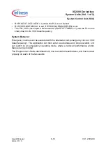
The following figure shows the PLL block structure.
Figure 6-5
PLL Block Diagram
Clock Source Control
The reference frequency
f
R
can be selected to be either taken from the trimmed current
controlled clock source
f
INT
or from an external clock source
f
IN
.
PLL _Block _Diagram.vsd
PLL Block
f
IN
Osc.
WDG
P-
Divider
VCO
Core
K2-
Divider
N-
Divider
Lock
Detect.
K1-
Divider
f
PLL
f
K2
f
K1
f
VCO
f
DIV
f
REF
f
P
f
R
PLLCON 1.
OSCSEL
PLLSTAT .
FINDIS
PLLCON0.
VCOBY
M
U
X
M
U
X
1
0
0
1
Clock
Source
f
INT
PLLSTAT .
VCOLOCK
HPOSCCON.
PLLV
PLLCON1.
RESLD
HPOSCCON.
OSCWDTRST


